Multichip package and fabrication method thereof

Active Publication Date: 2014-06-12
MAGNACHIP SEMICONDUCTOR LTD
View PDF26 Cites 2 Cited by
  • Summary
  • Abstract
  • Description
  • Claims
  • Application Information

AI Technical Summary

Benefits of technology

[0024]The lead frame connected to the control IC chip may be partially formed in a zigzag pattern.
[0025]The lead frames connected to the drains of the MOSFET chips each may have a greater width than each of the lead frames connected to sources of the MOSFET chips

Problems solved by technology

However, when a package is fabricated by simply arranging a plurality of semiconductor chips on a lead frame pad, thermal and/or electrical interference may occur among the neighboring chips within the package.
Because the lead frame pad is made from a metallic material, without a separate structure to insulate or isolate the chips from each other, thermal and/or electrical interference is generated.
Such thermal and/or electrical interferences may cause chips to malfunction, and may result in a defect in a prod

Method used


Image

  • Multichip package and fabrication method thereof
  • Multichip package and fabrication method thereof
  • Multichip package and fabrication method thereof

Examples


Embodiment Construction

[0040]The following detailed description is provided to assist the reader in gaining a comprehensive understanding of the methods, apparatuses, and / or systems described herein. Accordingly, various changes, modifications, and equivalents of the systems, apparatuses and / or methods described herein will be suggested to those of ordinary skill in the art. Also, descriptions of well-known functions and constructions may be omitted for increased clarity and conciseness.

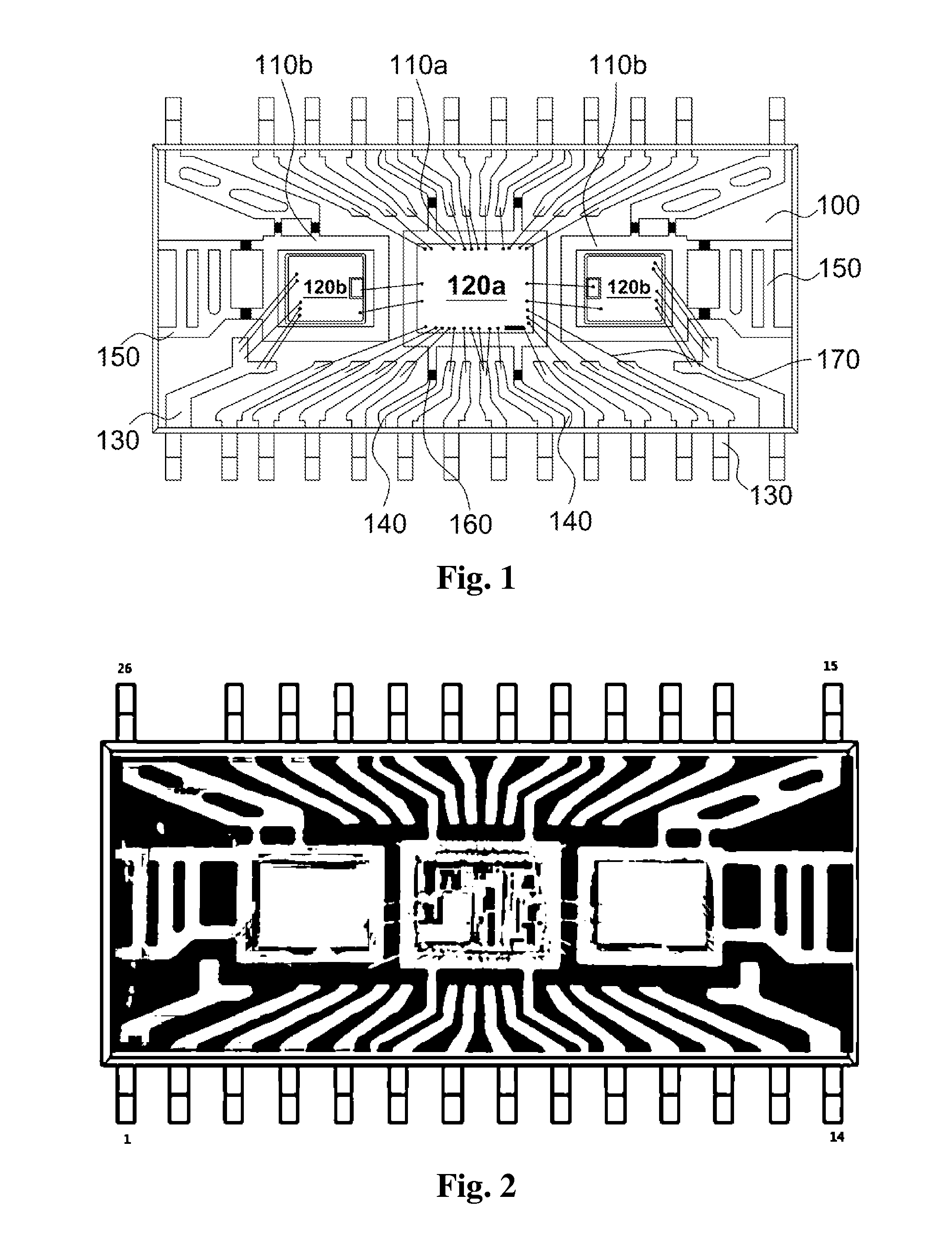
[0041]In an example, a multichip package may be constructed by adding a plurality of chips to a small outline package (SOP) and a quad flat package (QFP) provided on a surface of a printed circuit board (PCB) by using a surface mount technology (SMT). For instance, three SOP chips and four QFP chips may be arranged to construct a multichip package.

[0042]The ‘QFP’ as used herein refers to a package structure in which lead frames protrudes from the four corners. The ‘SOP’ as used herein refers to a package structure in which...


PUM


Abstract

A multichip package and a method for manufacturing the same are provided. A multichip package includes: a plurality of semiconductor chips each mounted on corresponding lead frame pads; lead frames connected to the semiconductor chips by a bonding wire; and fixed frames integrally formed with at least one of the lead frame pads and configured to support the lead frame pads on a package-forming substrate.

Description

CROSS-REFERENCE TO RELATED APPLICATIONS[0001]This application claims the benefit under 35 U.S.C. §119(a) of Korean Patent Application No. 10-2012-0141266, filed on Dec. 6, 2012, in the Korean Intellectual Property Office, the entire disclosure of which is incorporated herein by reference for all purposes.BACKGROUND[0002]1. Field[0003]The following description relates to a multichip package and a fabricating method thereof, and to, for example, a multichip package provided in a form of a single package in which a plurality of semiconductor chips are arranged in a small outline package (SOP) as a surface mount device or in a quad flat package (QFP).[0004]2. Description of Related Art[0005]Semiconductor chip packaging technologies are actively being researched, with efforts to reduce the overall size of the devices, and to increase the packaging densities of the devices. Packaging technologies relate to appropriate arrangements of semiconductor elements such as ICs and switching elemen...

Claims


Application Information

Patent Timeline
IPC IPC(8): H01L23/495H01L21/56
CPCH01L2224/32245H01L2224/48247H01L2224/48091H01L2224/48137H01L2224/73265H01L23/49541H01L23/49551H01L23/49562H01L2924/13091H01L21/565H01L2924/181H01L2924/00011H01L2224/45565H01L2224/45616H01L23/49537H01L2924/00014H01L2924/00H01L2224/45147H01L2924/00012H01L2924/01005H01L23/12H01L23/495H01L21/56H01L23/49555H01L23/49575H01L24/29H01L24/32H01L24/45H01L24/48H01L24/73H01L24/83H01L24/92H01L2224/2929H01L2224/29339H01L2224/48175H01L2224/83851H01L2224/92247H01L2924/0665
Inventor KIM, HYUN DONG
Owner MAGNACHIP SEMICONDUCTOR LTD
Why Eureka
Try Eureka