Charge distribution control for secure systems

Active Publication Date: 2014-06-19
CHAOLOGIX INC
View PDF8 Cites 29 Cited by
  • Summary
  • Abstract
  • Description
  • Claims
  • Application Information

AI Technical Summary

Benefits of technology

[0006]According to an embodiment, a clocked charging mechanism is provided that isolates a logic cell from a power supply and provides charge to the logic cell that does not present current leakage in a manner that could enable the states of the logic cell from being deciphered. The clocked charging mechanism for the logic cell inhibits a readout of a power signature for the logic cell by isolating both the high and low supply rail of the logic cell from external pads including a power supply voltage and ground connection.

Problems solved by technology

Attackers attempt to extract these keys from the card in order to modify the card's contents, create a duplicate card, or generate an unauthorized transaction.

Method used


Image

  • Charge distribution control for secure systems
  • Charge distribution control for secure systems
  • Charge distribution control for secure systems

Examples


example 1

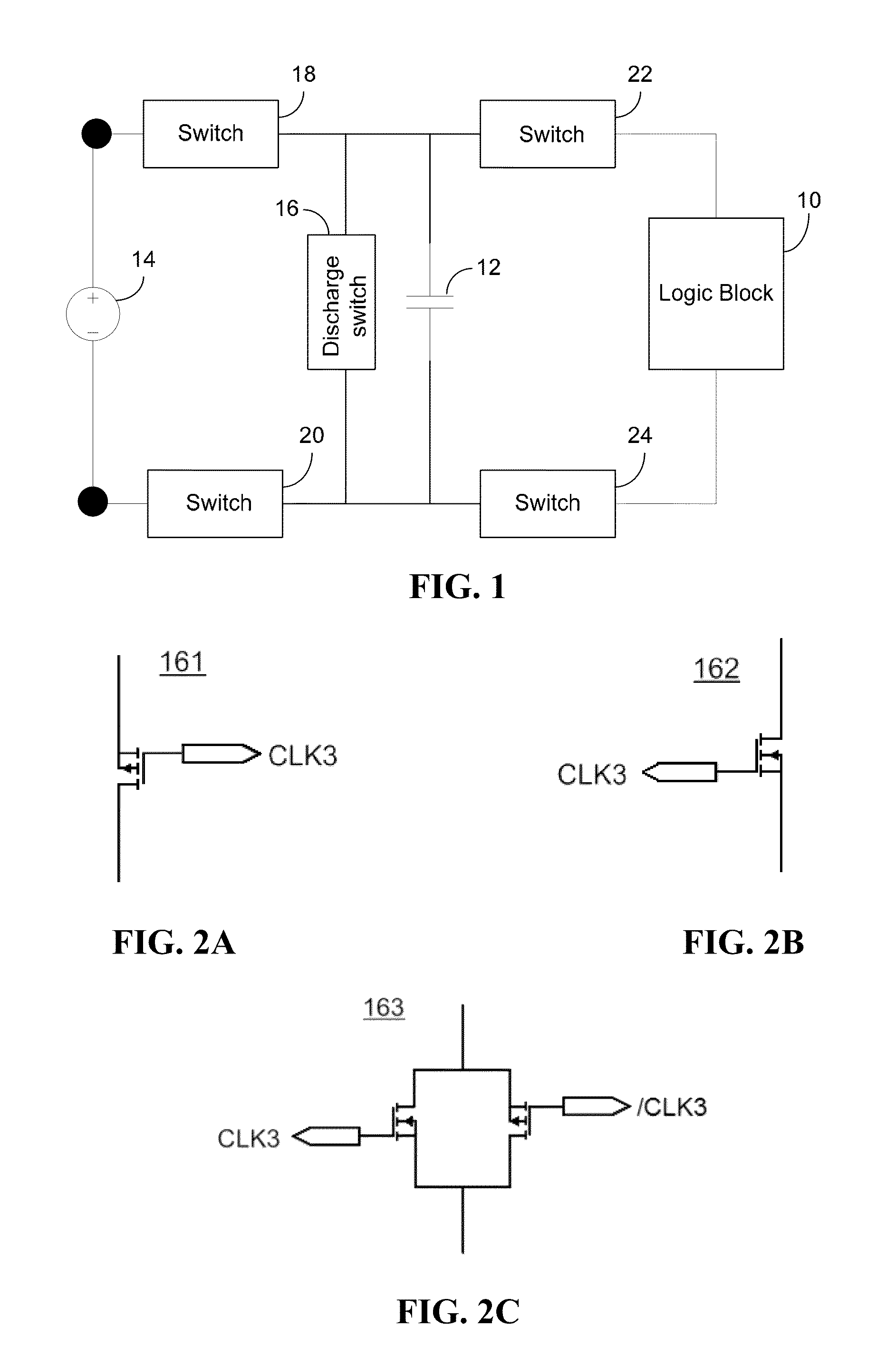
[0119]FIG. 4 is a schematic representation of an implementation of a CCDL circuit according to an embodiment of the invention. Referring to FIG. 4, MOSFETs M1, M2, M11, M12, and M13 are used to implement the switches seen in FIGS. 1 and 3A-3D. MOSFET M5 is used to implement the capacitor C1. MOSFETs M3, M4, M6, M7, M8, and M10 implement a static logic “AND gate.”

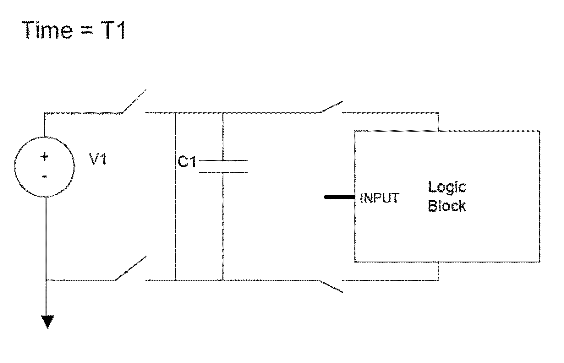
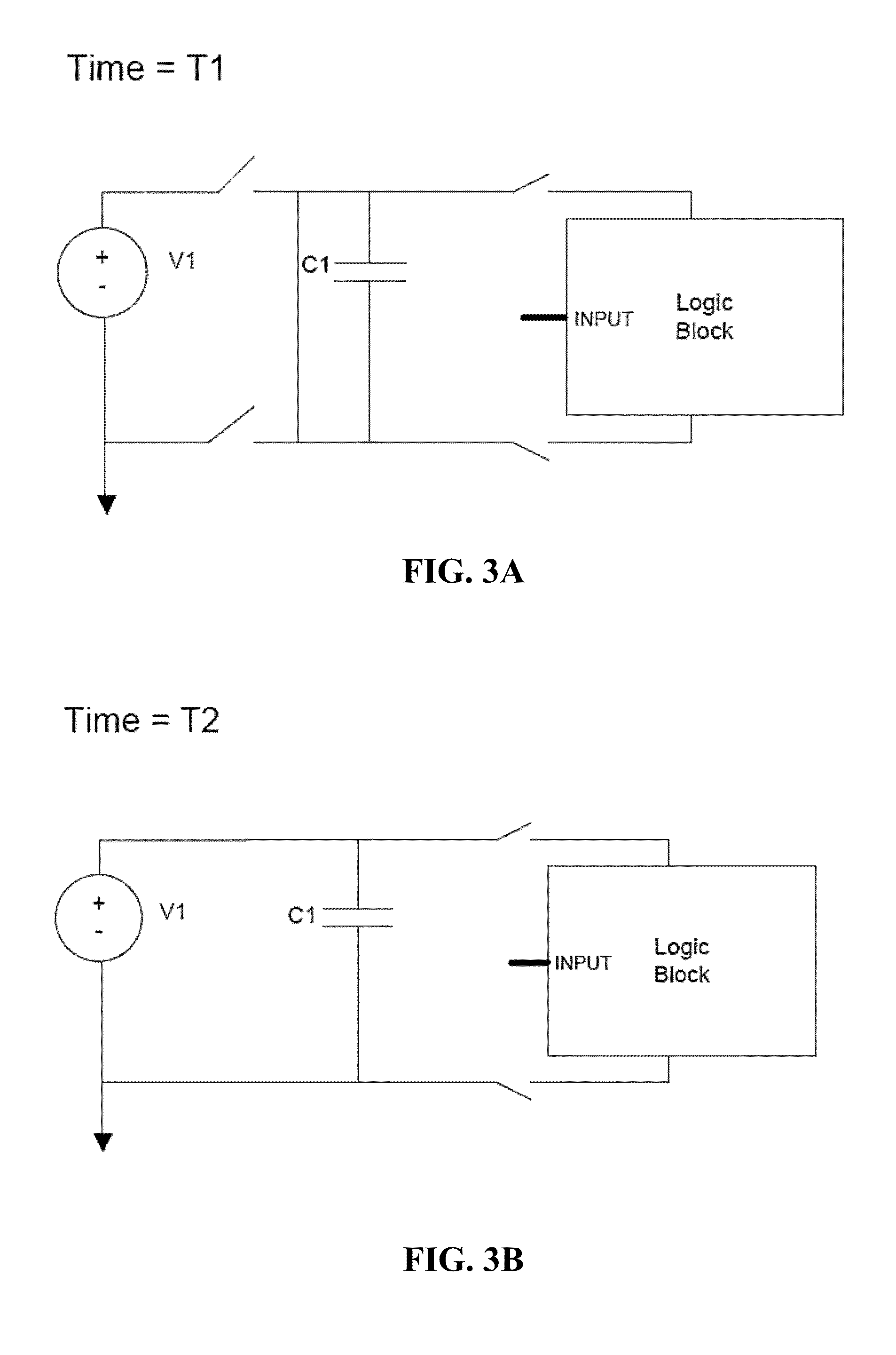
[0120]In a first phase, MOSFETs M1, M2, M11, and M12 are disabled (turned off) to decouple the logic block and the power supply from capacitor M5. Immediately following, M13 is enabled (turned on) to couple the gate of M5 to the source and drain terminals of M5, thereby allowing the M5 to discharge.

[0121]In a second phase, M2, M11, and M13 are disabled to decouple M5 from the logic block. MOSFETs M1 and M12 are then enabled to couple M5 to power supply lines VDD and VSS, thereby allowing M5 to charge.

[0122]In a third phase, MOSFETs M1, M12, and M13 are disabled to disconnect M5 from supply lines VDD and VSS. Immediately afte...

example 2

[0125]FIG. 5 shows a clocking scheme for a CCDL logic cell. The signal SL_CLK represents an input to a CCDL cell that would induce a logic transition. The transitioning of signals CLK1 and CLK1B disconnects the logic block from the supply capacitor and the power supply. The limiting factor in determining the max operation speed of a CCDL cell or a CCDL based circuit block is the necessity for all logic transitions within the CCDL block to be complete before CLK1 and CLK1B signals disconnect the logic block within the CCDL cells from the supply capacitor powering the logic blocks.

[0126]Once the CLK1 and CLK1B signals have decoupled the logic block from the supply capacitor, CLK3 can transition and discharge the supply capacitor. Finally, CLK2 and CLK2B signals transition to allow the supply capacitor to be charged by the power supply. It should be noted that, the transition edges of each of the CLK signals do not overlap. The non-overlapping clocks inhibit, for example, the power sup...

example 3

[0127]A CCDL cell as shown in FIG. 6 was tested. The discharge switch for the cell in this example utilizes a transmission gate of NMOS transistor M13 and PMOS transistor M14. Testing of the CCDL cells within a larger circuit demonstrated a small but significant level of current, i.e., tens of micro amps, flowing through the substrate of the circuit and into the power supply during switching events of the CCDL logic. Although small, some level of information may have been extractable from these currents about the logical operations of the CCDL circuit. Two approaches were implemented to reduce this. First, the body tie of each device in the CCDL logic cell (circled on the right) was tied to the internal supply rails of the CCDL cell, i.e., CP_RL and CP_GND. This attempts to flow as much of the substrate current generated during logic operations as possible into, and / or out of, the power capacitor.

[0128]The second approach used to reduce current on power and ground lines is shown in ...


PUM


Abstract

Advantageous analog and / or digital logic cells and methods of powering circuit blocks using the same are provided. A digital logic cell can include a charge storage device, a logic block, and connections to a power supply. The charge storage device may be a capacitor. The capacitor or other charge storage device can be disconnected from the logic block and a power supply to discharge the capacitor, and then connected to the power supply, via the power supply connections, to charge the capacitor. The capacitor can be disconnected from a ground connection of the power supply while the capacitor is discharged. After being charged via the power supply, the capacitor can also be disconnected from the power supply (including ground) and connected to the logic block to power the logic block.

Description

CROSS-REFERENCE TO RELATED APPLICATIONS[0001]The present application is a continuation-in-part of U.S. application Ser. No. 13 / 906,542, filed May 31, 2013, which claims the benefit of U.S. Provisional Application Ser. No. 61 / 725,128, filed Nov. 12, 2012, which are hereby incorporated by reference in their entirety, including any figures, tables, or drawings.BACKGROUND[0002]There are many secure applications in which it can be important to protect electronically stored and / or processed data. Secure applications are implemented today in many areas, including ATM cards, identification cards, stored value cards, credit cards, cellular telephones (e.g., SIM cards), computer access control, pay TV, and storage of medical information. Security for these cards and applications often rely on cryptographic computations based on secret keys embedded in the memories of the cards (or other circuitry). Attackers attempt to extract these keys from the card in order to modify the card's contents, c...

Claims


Application Information

Patent Timeline
Patent Type & Authority Applications(United States)
IPC IPC(8): H03K19/003
CPCH03K19/003H03K19/17768G06F21/725G06F21/74H04L9/002H04L2209/12G09C1/00G06F21/755H03K19/00315H03K19/0948Y04S40/20G06F21/81G06F2221/034
Inventor YANNETTE, DANIEL F.MYERS, BRENT ARNOLD
Owner CHAOLOGIX INC
Why Eureka
Try Eureka