Semiconductor device

a technology of semiconductors and devices, applied in the direction of basic electric elements, casings/cabinets/drawers, casings/cabinets/drawers details, etc., can solve the problems of difficult to accurately position and fix and the accuracy of the control terminal b>54/b> is difficult, so as to achieve the effect of high degree of accuracy and highly accurate determination of the position of the control terminal

Active Publication Date: 2014-06-19
FUJI ELECTRIC CO LTD
View PDF4 Cites 4 Cited by
  • Summary
  • Abstract
  • Description
  • Claims
  • Application Information

AI Technical Summary

Benefits of technology

[0019]According to the present invention, because the two projections provided on a side end surface of the control terminal are fitted to the convex step portion of the resin block that is inserted into the opening of the resin case, the control terminal can be fixed to the resin case so as not to be moved by external force. Hence, even when external force such as a compressive load or tensile load is applied to the control terminal, the control terminal can be prevented from sinking into the resin case or being pulled out of the resin case.
[0020]Further, according to the present invention, as a result of holding the control terminal between the side surface of the resin block and the sidewall of the opening of the resin case and fitting the convex step portion of the resin block into the valley between the two projections of the control terminal, the control terminal can be fixed in place in the resin case. Thus, the position of the control terminal can be determined highly accurately.
[0021]The semiconductor device and the method of manufacturing the same according to the present invention exerts the effect of fixing the control terminal to the resin case without causing vertical movement of the control terminal, even when a compressive load or tensile load is applied to the control terminal. The semiconductor device and the method of manufacturing the same according to the present invention can also exert the effect of positioning the control terminal with a high degree of accuracy.

Problems solved by technology

A problem with the conventional IGBT module shown in FIG. 19 is that the control terminal 54 sinks into the resin case 55 when a compressive load is applied to the control terminal 54.
Another problem is that a tensile load applied to the control terminal 54 tears the joint between the control terminal and the patterned insulating substrate 52, pulling the control terminal 54 out of the resin case 55.
Because this conventional structure allows the control terminal 34 to move easily, it is difficult to highly accurately position and fix the control terminal 54 in the resin case 55.
The control terminal 54 is deformed easily especially when the arm portion thereof is long, making an accurate positioning of the control terminal 54 more difficult.

Method used


Image

  • Semiconductor device
  • Semiconductor device
  • Semiconductor device

Examples


embodiment 1

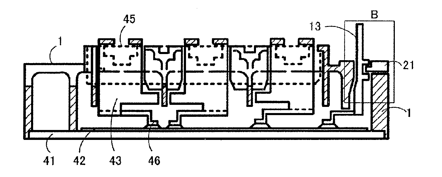
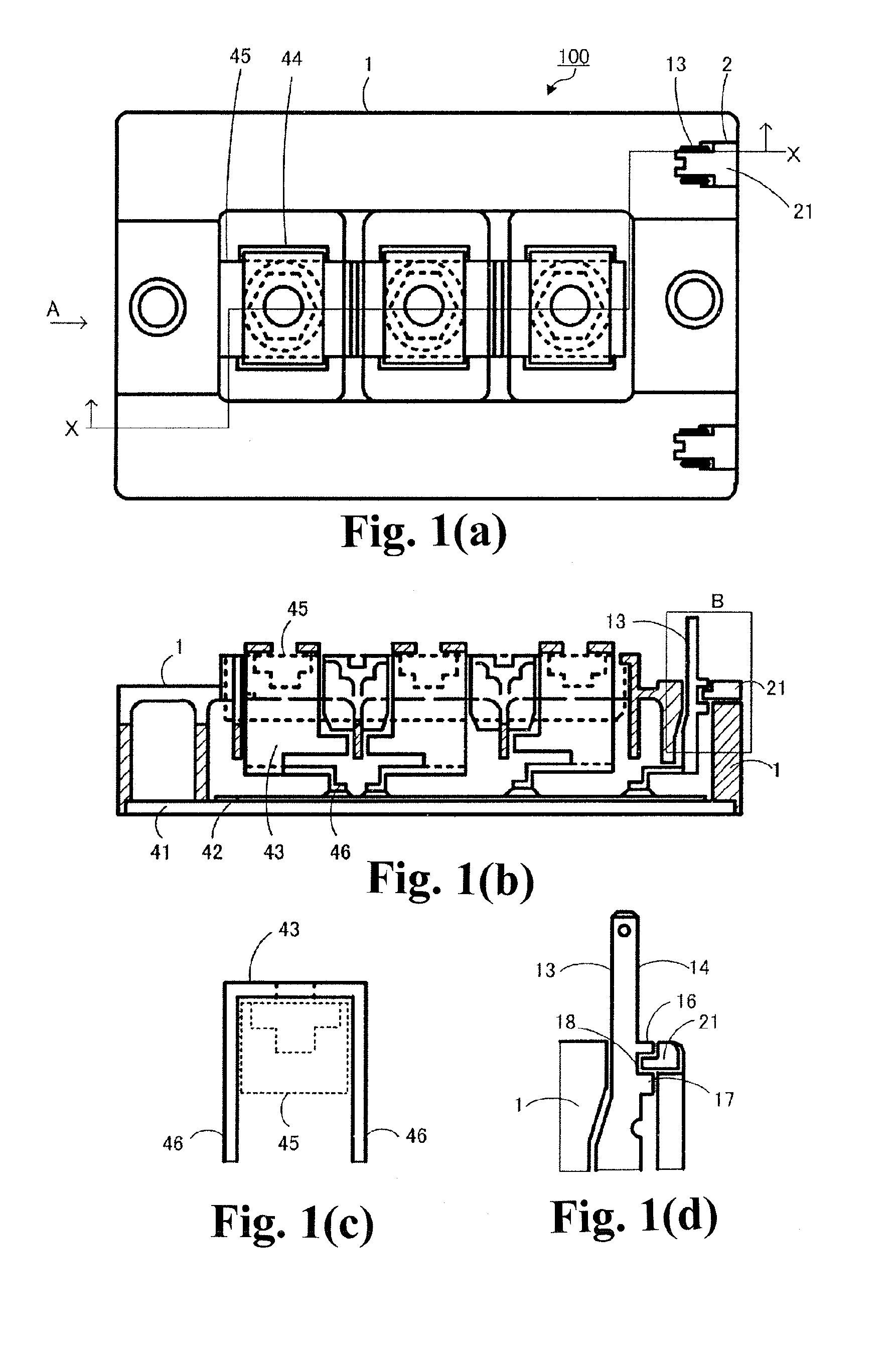
[0042]The configurations of the semiconductor device according to the present invention are described with reference to FIGS. 1(a) to 6. FIGS. 1(a)-1(d) are explanatory diagrams showing the configurations of substantial parts of a semiconductor device according to Embodiment 1 of the present invention. FIG. 1(a) is a top view of the semiconductor device 100 according to Embodiment 1. FIG. 1(b) is a side view taken along the line X-X of FIG. 1(a). FIG. 1(c) is a front view of a main terminal 43 which is viewed in the direction of the arrow A shown in FIG. 1(a). FIG. 1(d) is a cross-sectional diagram showing the detail of a rectangular section B shown in FIG. 1(b). This semiconductor device 100 is, for example, an IGBT module.

[0043]As shown in FIGS. 1(a)-1(d), the semiconductor device 100 has a resin case 1, a heat dissipating base 41, a patterned insulating substrate 42, a nut globe 45, a main terminal 43, a control terminal 13, and a resin block 21. The patterned insulating substrat...

embodiment 2

[0068]The method of manufacturing a semiconductor device according to the present invention is now described in detail. FIGS. 7(a) to 10(b) are each an explanatory diagram showing a semiconductor device of Embodiment 2 of the present invention in process of manufacture. The method of manufacturing a semiconductor device according to Embodiment 2 is a method of manufacturing the semiconductor device 100 of Embodiment 1 shown in FIGS. 1(a) to 6. Throughout FIGS. 7(a) to 10(b), (a) is a cross-sectional diagram showing the entire semiconductor device 100, and (b) is an enlarged plan view showing the area near the control terminal 13.

[0069]As shown in FIGS. 7(a), 7(b), a semiconductor chip (not shown), the main terminal 43, and the control terminal 13 are fixated onto the patterned insulating substrate 42 by means of soldering (or sometimes welding), the patterned insulating substrate 42 being fixated onto the heat dissipating base 41. Next, the resin case 1 is installed so as to cover t...

embodiment 3

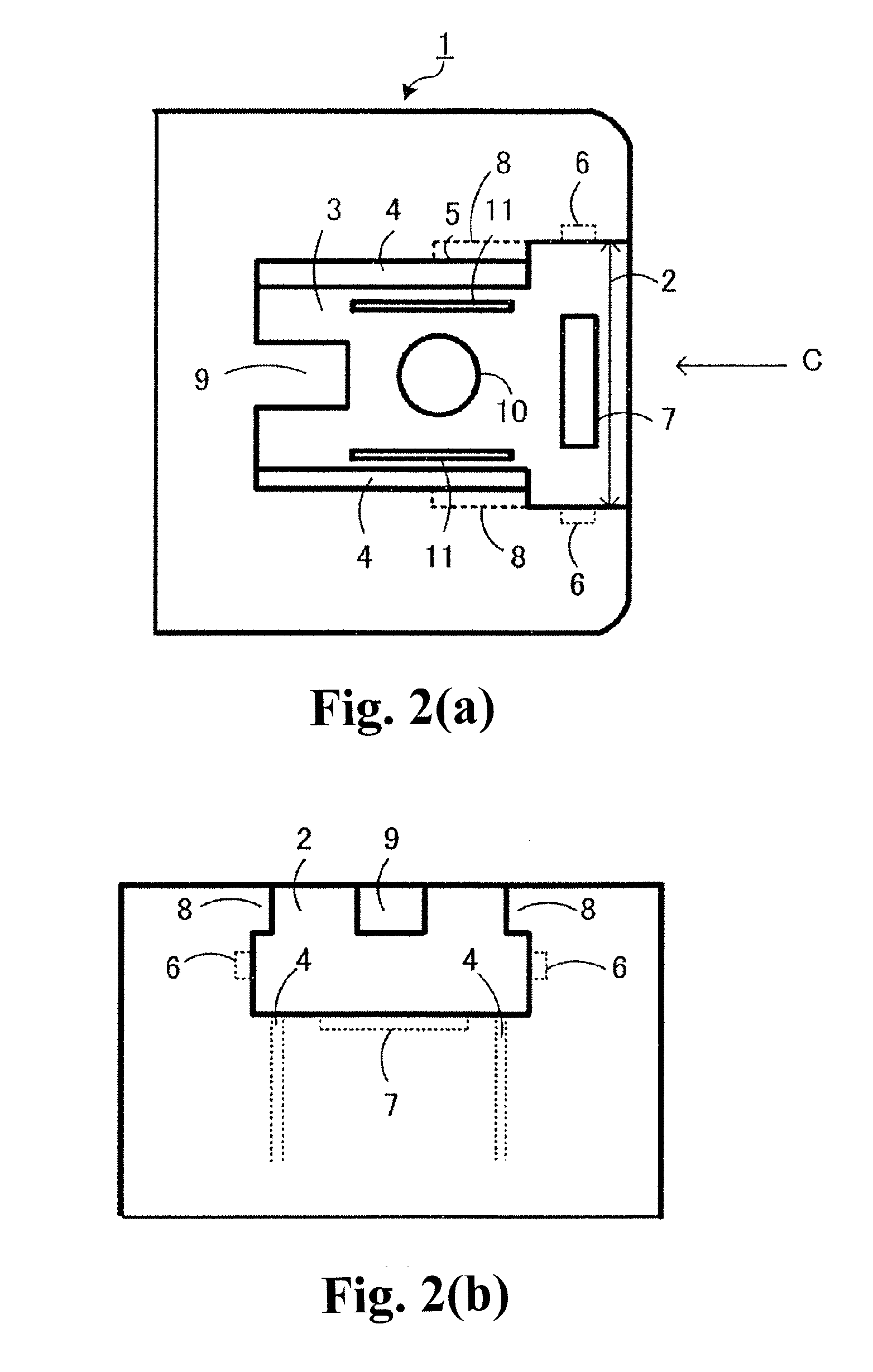
[0073]Another configuration of the semiconductor device of the present invention is now described as Embodiment 3 with reference to FIGS. 11(a), 11(b) and 12(a)-12(c). FIGS. 11(a), 11(b) and 12(a)-(c) are each an explanatory diagram showing the configurations of substantial parts of a semiconductor device according to Embodiment 3 of the present invention. The semiconductor device according to Embodiment 3 is a modification of the semiconductor device of Embodiment 1 shown in FIGS. 1(a) to 6. FIGS. 11(a), 11(b) show the other configurations of substantial parts near the control terminal of the resin case shown in FIG. 1. FIG. 11(a) is a plan view of the resin case 1. FIG. 11(b) is a front view of the resin case 1, showing FIG. 11(a) in the direction of the arrow E. FIGS. 12(a)-12(c) show the other configurations of the resin block by which the control terminal shown in FIGS. 1(a)-1(d) is positioned and fixed. FIG. 12(a) is a plan view of the resin block 21. FIG. 12(b) is a bottom vi...


PUM


Abstract

A semiconductor device has a control terminal attached to a patterned insulating substrate; a first projection formed on the control terminal; a second projection formed on the control terminal; a concave formed between the first projection and the second projection; a resin case disposed to cover the patterned insulating substrate, and having an opening for passing the control terminal therethrough; a first concave portion; a beam portion disposed at the opening of the resin case; a second concave portion formed in the beam portion; a resin block inserted into the opening of the resin case and sandwiching the control terminal together with the sidewall of the opening of the resin case to fix the control terminal to the resin case; a convex step portion; a third projection formed on a side surface of the resin block; and a fourth projection thinned on a bottom surface of the resin block.

Description

TECHNICAL FIELD[0001]The present invention relates to a semiconductor device in which a control terminal can highly accurately be fixed to a resin case, and a method of manufacturing such a semiconductor device.BACKGROUND ART[0002]A conventional IGBT module has been known in which a main terminal and a control terminal, which are external lead terminals, are soldered onto a conductive pattern (circuit pattern) formed on an insulating substrate (referred hereinafter as “patterned insulating substrate”) (see Patent Document 1 below, for example). Patent Document 1 uses independent terminals as the external lead terminals. The independent terminals are not fixed to a resin case, wherein they are not insert-molded into a resin case. The independent terminals are electrically connected to external wiring by nut globes which are resin structures of nuts and nut receivers fitted together.[0003]With the recent increase in the integration density of an IGBT module, the joint between the patt...

Claims


Application Information

Patent Timeline
Patent Type & Authority Applications(United States)
IPC IPC(8): H05K5/02
CPCH05K5/0247H01L25/072H01L23/049H01L23/49811H01L23/3735H01L2224/291H01L2224/32225H01L2924/13055H01L2924/1305H01L2924/014H01L2924/00H01L21/56H01L23/053H01L23/10H01L23/147H01L23/29H01L23/3121H01L23/3142H01L23/315H01L23/34H01L23/36H01L23/544H01L29/66325
Inventor KODAIRA, YOSHIHIRO
Owner FUJI ELECTRIC CO LTD
Why Eureka
Try Eureka