Optoelectronic device comprising three-dimensional semiconductor elements and method for the production thereof

a technology of three-dimensional semiconductor elements and optoelectronic devices, which is applied in the direction of semiconductor devices, basic electric elements, electric devices, etc., can solve the problems of altering the efficiency of the conversion of electric signals into electromagnetic radiation or the other way, and the growth of nanowires may be disturbed, so as to achieve accurate and uniform control of position, crystallographic properties, and crystallographic properties.

Inactive Publication Date: 2017-12-21
COMMISSARIAT A LENERGIE ATOMIQUE ET AUX ENERGIES ALTERNATIVES
View PDF0 Cites 0 Cited by
  • Summary
  • Abstract
  • Description
  • Claims
  • Application Information

AI Technical Summary

Benefits of technology

[0013]Another object of an embodiment of the present invention is the possibility to accurately and uniformly control the position, the geometry, and the crystallographic properties of each three-dimensional element, especially of each microwire or nanowire, made of semiconductor material.
[0014]Another object of an embodiment of the present invention is the possibility to form the three-dimensional elements, and especially the microwires or nanowires, made of semiconductor material, at an industrial scale and at low cost.

Problems solved by technology

However, with the method disclosed in U.S. Pat. No. 7,829,443, the nanowire growth may be disturbed, so that each nanowire might not have a single-crystal structure.
This may cause the forming of defects, especially at grain boundaries, which may alter the efficiency of the conversion of an electric signal into electromagnetic radiation or the other way.

Method used


Image

  • Optoelectronic device comprising three-dimensional semiconductor elements and method for the production thereof
  • Optoelectronic device comprising three-dimensional semiconductor elements and method for the production thereof
  • Optoelectronic device comprising three-dimensional semiconductor elements and method for the production thereof

Examples


Embodiment Construction

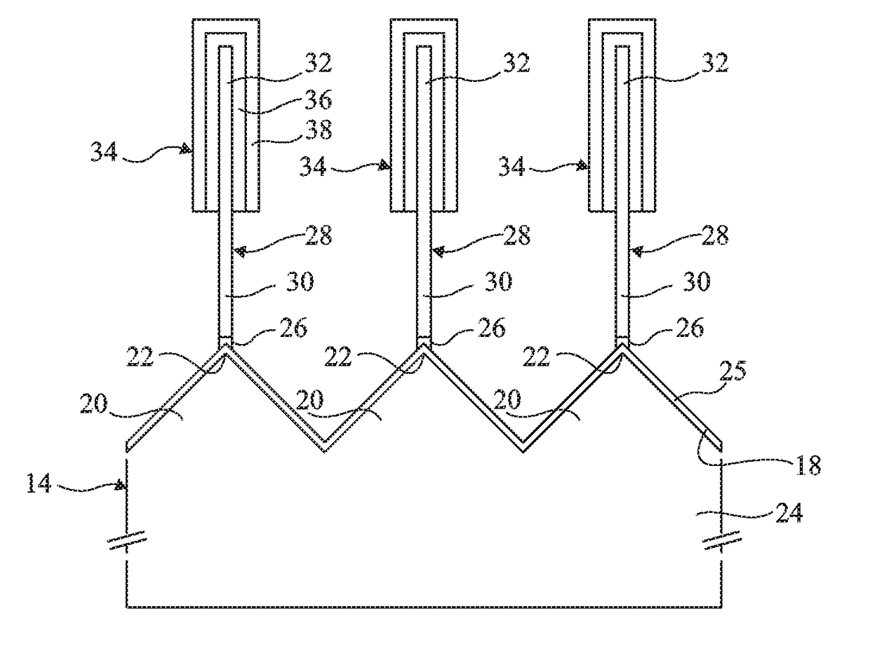
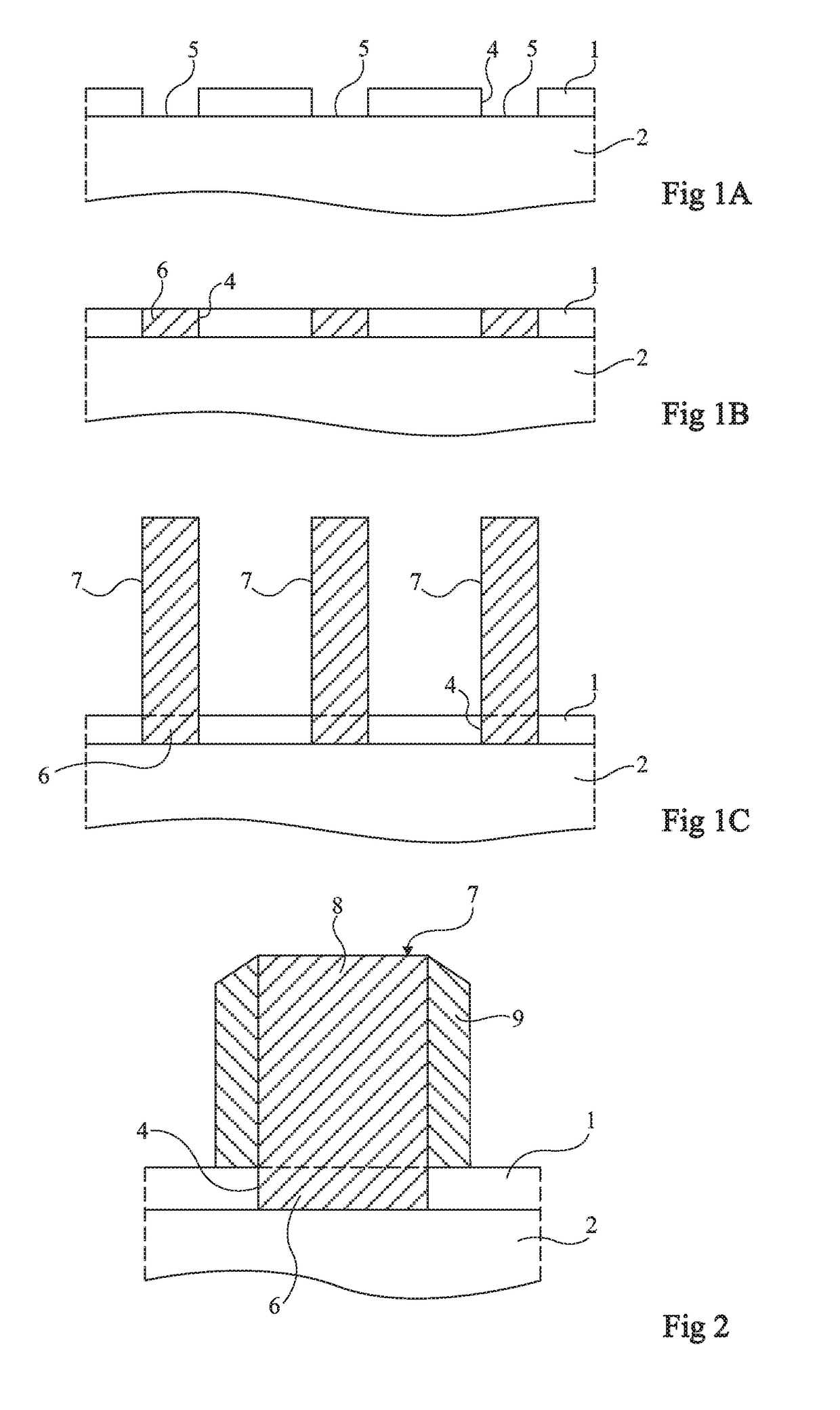
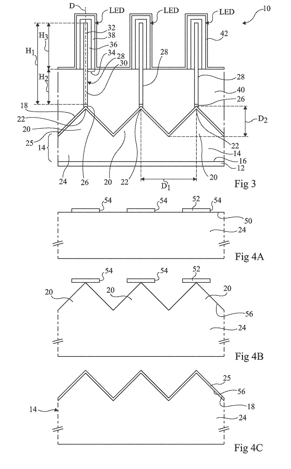
[0037]For clarity, the same elements have been designated with the same reference numerals in the various drawings and, further, as usual in the representation of electronic circuits, the various drawings are not to scale. Further, only those elements which are useful to the understanding of the present description have been shown and will be described. In particular, the optoelectronic device biasing and control means are well known and will not be described. In the following description, unless otherwise indicated, terms “substantially”, “approximately”, and “in the order of” mean “to within 10%”, preferably to within 5%.

[0038]In the following description, saying that a compound based on at least one first element and on a second element has a polarity of the first element and a polarity of the second element means that the material grows along a preferred direction and that when the material is cut in a plane perpendicular to the preferred growth direction, the exposed surface es...


PUM

PropertyMeasurementUnit
diameteraaaaaaaaaa
distanceaaaaaaaaaa
temperatureaaaaaaaaaa

Abstract

An optoelectronic device including a carrier having a face including flat butt-jointed facets inclined in relation to each other; seeds, mainly made of a first compound selected from the group including the compounds III-V, the compounds II-VI, and the compounds IV, in contact with the carrier in the region of at least some of the joints between the facets; and conical or frustoconical, wire-like three-dimensional semiconductor elements of a nanometric or micrometric size, mainly made of the first compound, on the seeds.

Description

[0001]The present patent application claims the priority benefit of French patent application FR14 / 61345 which is herein incorporated by reference.BACKGROUND[0002]The present disclosure generally relates to optoelectronic devices comprising three-dimensional semiconductor elements, for example, microwires, nanowires, conical elements, or frustoconical elements, and to methods of manufacturing the same.[0003]Term “optoelectronic devices” is used to designate devices capable of converting an electric signal into an electromagnetic radiation or the other way, and especially devices dedicated to detecting, measuring, or emitting an electromagnetic radiation or devices dedicated to photovoltaic applications.DISCUSSION OF THE RELATED ART[0004]Microwires or nanowires based on a component mainly containing a group-III element and a group-V element (for example, gallium nitride GaN), called III-V compound hereafter, or mainly containing a group-II element and a group-VI element (for example,...

Claims


Application Information

Patent Timeline
Patent Type & Authority Applications(United States)
IPC IPC(8): H01L33/00H01L33/42H01L33/32H01L33/24H01L33/22H01L33/06H01L31/0216H01L31/18H01L31/0352H01L31/0304H01L31/0236H01L31/0224H01L33/44H01L33/08
CPCH01L33/0075H01L31/1856H01L33/08H01L33/22H01L33/24H01L33/32H01L33/44H01L33/42H01L31/035227H01L31/02366H01L31/035281H01L31/03044H01L31/02161H01L31/022466H01L33/06H01L21/0254H01L21/02576H01L21/02603H01L21/0262H01L21/02645H01L33/18H01L33/20H01L33/005
Inventor DUSSAIGNE, AMELIEBONO, HUBERT
Owner COMMISSARIAT A LENERGIE ATOMIQUE ET AUX ENERGIES ALTERNATIVES
Why Eureka
Try Eureka