Semiconductor integrated circuit and multi-chip package including the same

a technology of integrated circuits and semiconductors, applied in semiconductor devices, semiconductor/solid-state device testing/measurement, semiconductor/solid-state device details, etc., can solve the problems of high-speed operation and different kinds of noise, difficult to form bumps on probe pads, and difficult to bring probe pins into contact with bumps having a small size, so as to minimize the influence of probe test operation on other circuits and stable circuit operation

Inactive Publication Date: 2014-06-26
SK HYNIX INC
View PDF1 Cites 7 Cited by
  • Summary
  • Abstract
  • Description
  • Claims
  • Application Information

AI Technical Summary

Benefits of technology

[0022]In the semiconductor integrated circuit in accordance with one embodiment of the present invention, the influence of a probe test operation on other circuits may be minimized because the probe pad for the probe test operation is disposed at a predetermined place.
[0023]Furthermore, the MCP in accordance with one embodiment of the present invention may guarantee a stable circuit operation when performing a normal operation because a bump is stably formed although a probe pad may be damaged when performing a probe test operation.

Problems solved by technology

If wire bonding is used, however, there are disadvantages in terms of a high-speed operation and different kinds of noises.
When performing a test operation using a probe pin (hereinafter referred to as a ‘probe test operation’), however, it may be difficult to bring the probe pin into contact with the bump having a small size.
If the probe pad 120 is damaged, it may be difficult to form a bump on the probe pad 120.

Method used


Image

  • Semiconductor integrated circuit and multi-chip package including the same
  • Semiconductor integrated circuit and multi-chip package including the same
  • Semiconductor integrated circuit and multi-chip package including the same

Examples


Embodiment Construction

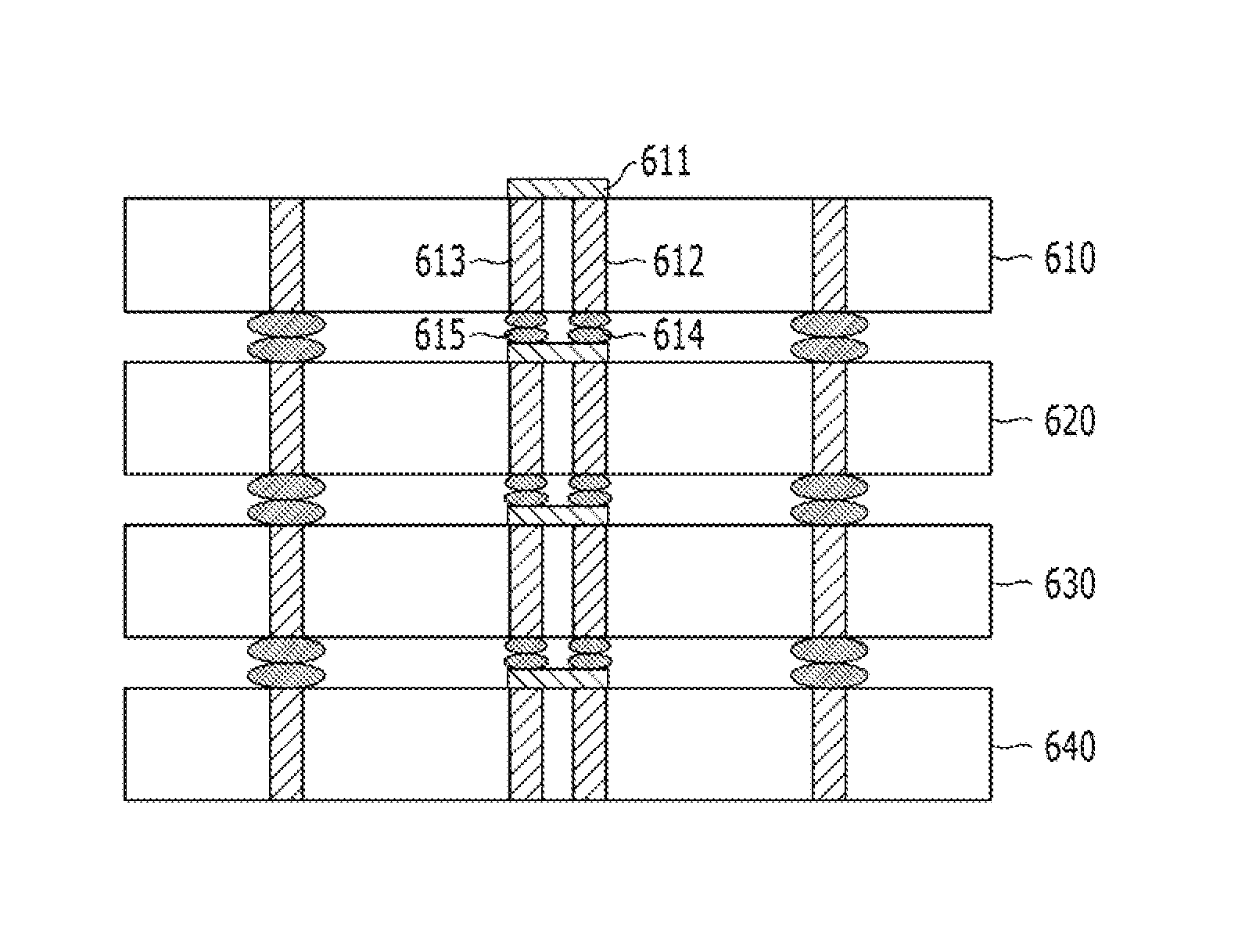
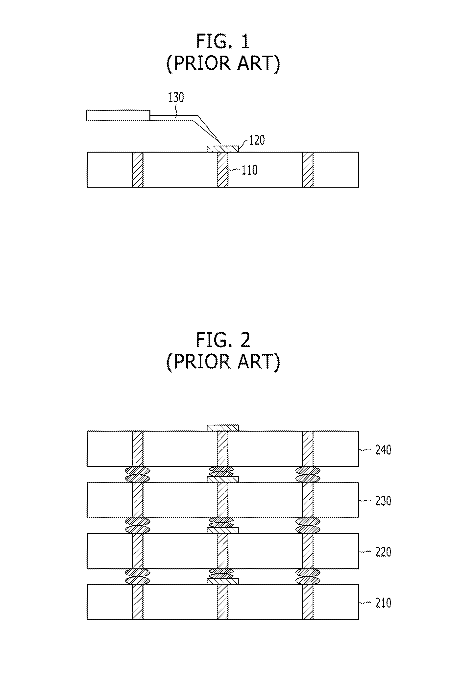
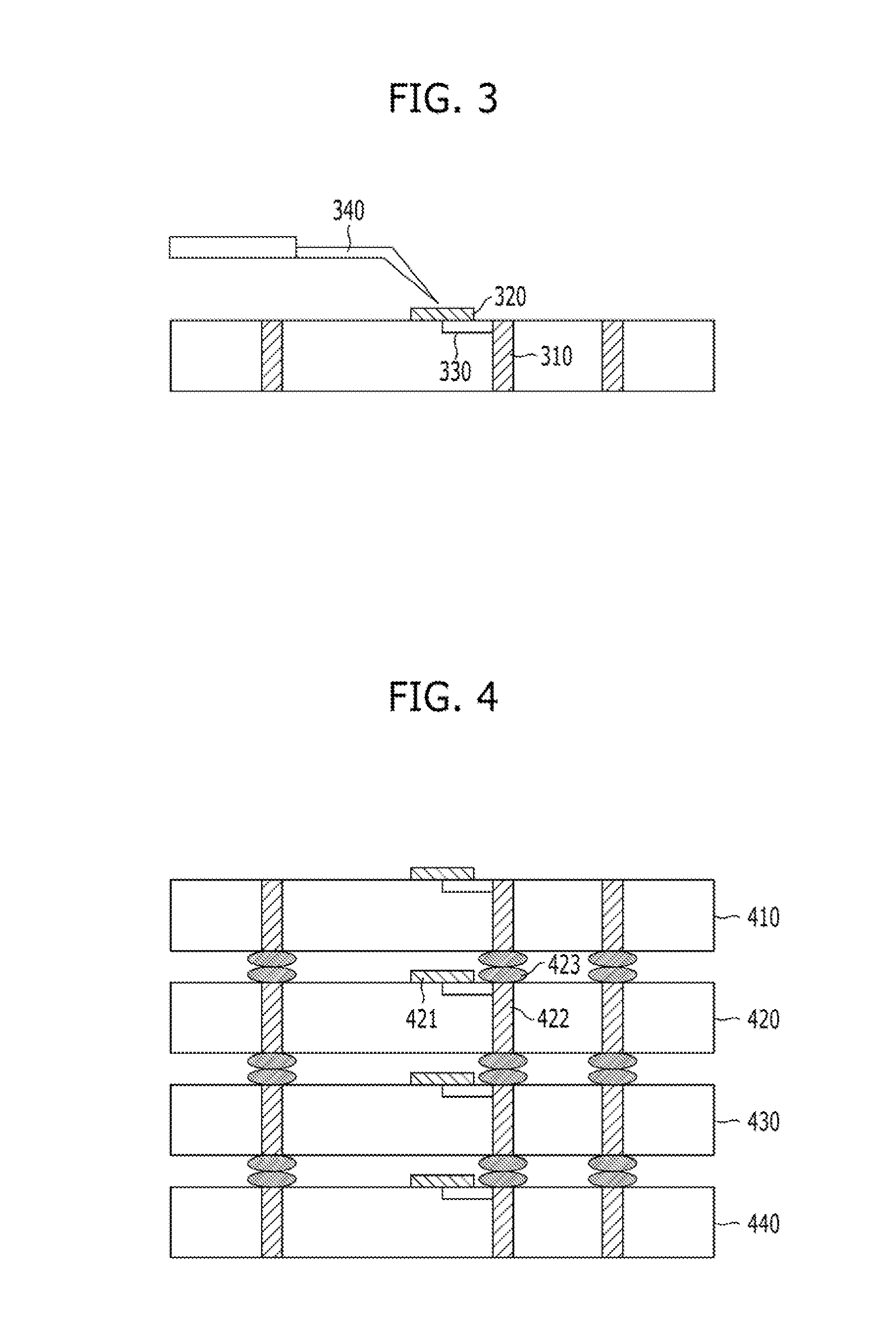
[0032]Exemplary embodiments of the present invention will be described below in more detail with reference to the accompanying drawings. The present invention may, however, be embodied in different forms and should not be construed as limited to the embodiments set forth herein, Rather, these embodiments are provided so that this disclosure will be thorough and complete, and will fully convey the scope of the present invention to those skilled in the art. Throughout the disclosure, like reference numerals refer to like parts throughout the various figures and embodiments of the present invention. It should be readily understood that the meaning of “on” and “over” in the present disclosure should be interpreted in the broadest manner such that “on” means not only “directly on” but also “on” something with an intermediate feature(s) or a layer(s) therebetween, and that “over” means not only directly on top but also on top of something with an intermediate feature(s) or a layer(s) ther...


PUM


Abstract

In an aspect of the present invention, a semiconductor integrated circuit includes a semiconductor chip including a through-chip via, a probe pad disposed in such a way as not to overlap with the through-chip via, and a connection part electrically coupling the probe pad and the through-chip via

Description

CROSS-REFERENCE TO RELATED APPLICATIONS[0001]The present application claims priority of Korean Patent Application No. 10-2012-0149782, filed on Dec. 20, 2012, which is incorporated herein by reference in its entirety.BACKGROUND[0002]1. Field[0003]Exemplary embodiments of the present invention relate to semiconductor design technology, and more particularly, to a semiconductor integrated circuit capable of providing a probe test and a multi-chip package (hereinafter referred to as an ‘MCP’) including the same.[0004]2. Description of the Related Art[0005]In general, a semiconductor device, such as double data rate synchronous DRAM (DDR SDRAM), is developing in different kinds of directions in order to satisfy the needs of users. One of the developing directions includes package technology. There is being proposed an MCP as package technology for semiconductor devices, The MCP refers to forming a plurality of semiconductor chips into one chip. The capacity of memory may be increased us...

Claims


Application Information

Patent Timeline
Patent Type & Authority Applications(United States)
IPC IPC(8): H01L21/66
CPCH01L22/32H01L2224/05569H01L24/16H01L24/13H01L2224/16145H01L2225/06513H01L2224/14181H01L24/14H01L2225/06541H01L2224/13025H01L2225/06565H01L2224/0401H01L2224/02372H01L2225/06596H01L2224/0557H01L2924/00014H01L24/05H01L25/0657H01L2224/05552H01L23/50H01L23/544
Inventor LEE, TAE-YONG
Owner SK HYNIX INC
Why Eureka
Try Eureka