Semiconductor device and method of manufacturing the same

a semiconductor and semiconductor technology, applied in semiconductor devices, semiconductor/solid-state device details, electrical devices, etc., can solve the problems of no longer having increased degree of integration, difficult to form pad portions, and physical limits of two-dimensional memory devices in which memory cells are fabricated in a single layer over a silicon substrate. achieve the effect of easy formation of pad portions

Active Publication Date: 2014-07-10
SK HYNIX INC
View PDF1 Cites 347 Cited by
  • Summary
  • Abstract
  • Description
  • Claims
  • Application Information

AI Technical Summary

Benefits of technology

[0008]Various embodiments relate to a semiconductor device capable of easily forming a pad portion and a method of manufacturing the same.

Problems solved by technology

Two-dimensional memory devices in which memory cells are fabricated in a single layer over a silicon substrate have reached physical limits and may no longer have increased degrees of integration.
It is difficult to form pad portions on word lines stacked on top of one another and form contact plugs so that the contact plugs are coupled to the pad portions.

Method used


Image

  • Semiconductor device and method of manufacturing the same
  • Semiconductor device and method of manufacturing the same
  • Semiconductor device and method of manufacturing the same

Examples


Embodiment Construction

[0019]Hereinafter, various embodiments of the present invention will be described with reference to the accompanying drawings. In the drawings, a thickness and a distance of components may be exaggerated compared to an actual physical thickness and interval for convenience of illustration. In the following description, detailed explanations of known related functions and constitutions may be omitted to avoid unnecessarily information obscuring the subject manner of the present invention. Like reference numerals refer to like elements throughout the specification and drawings.

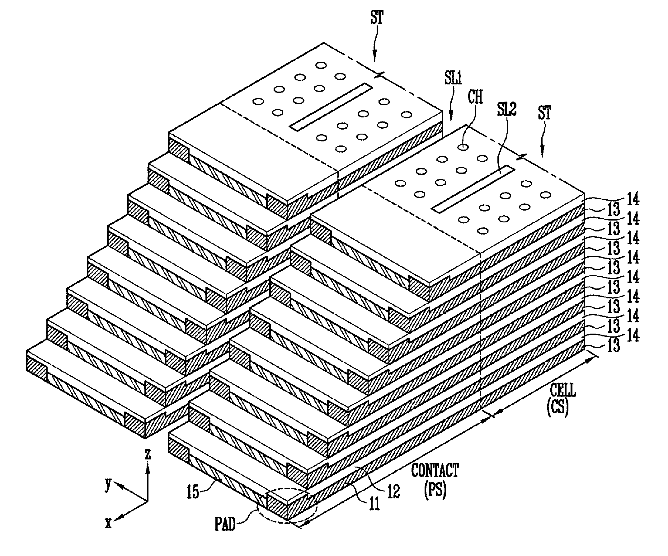
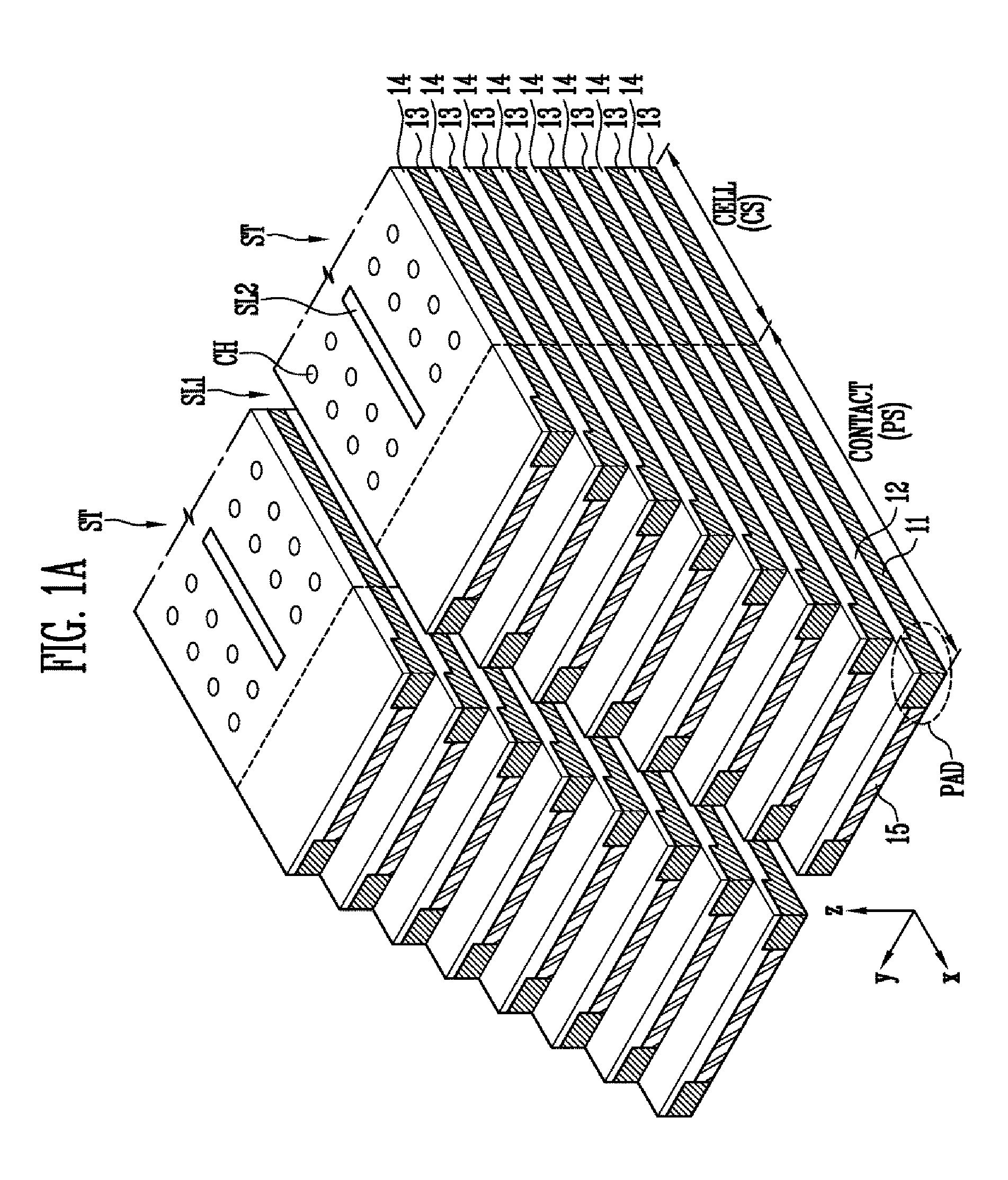
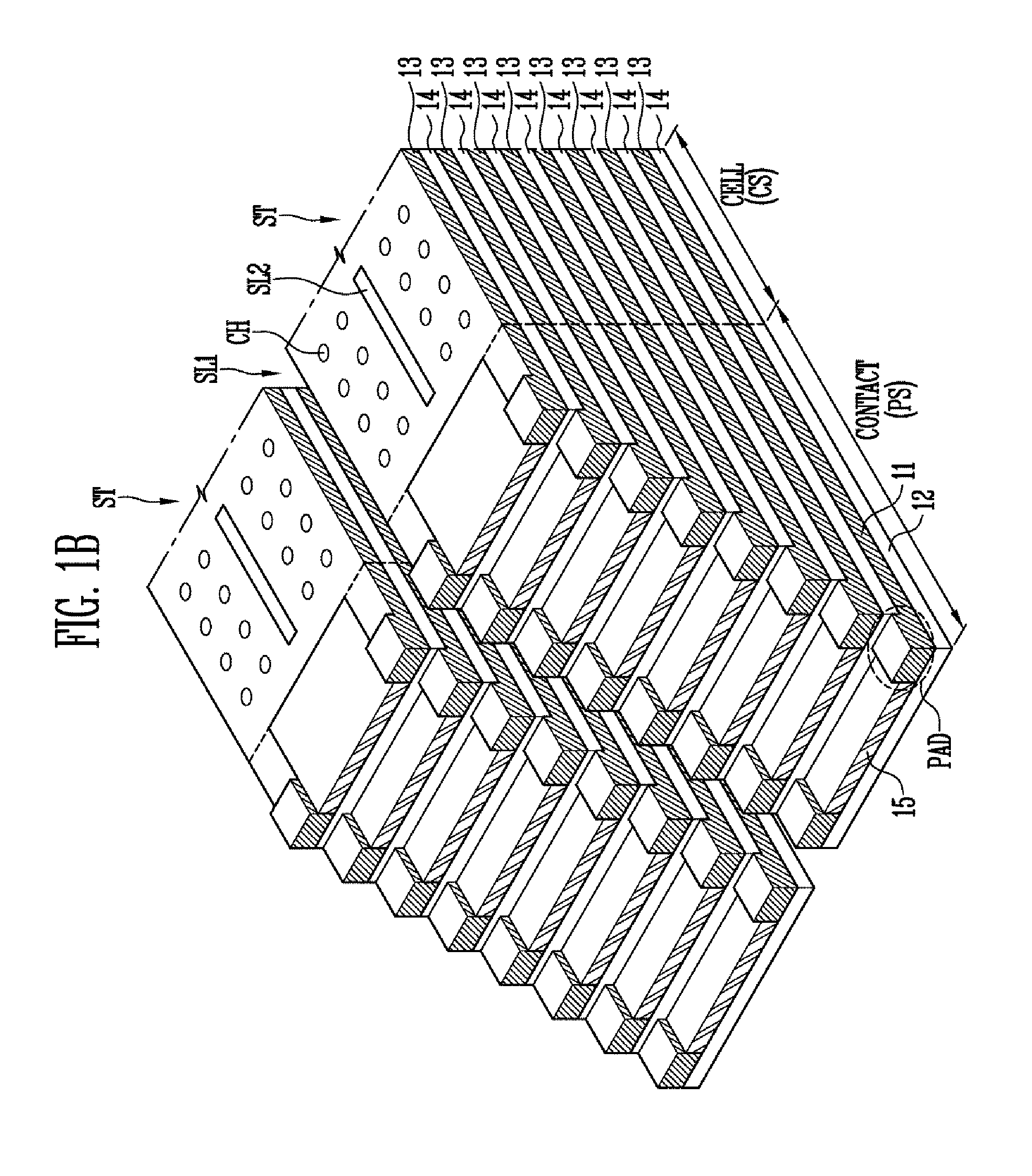
[0020]As illustrating in FIG. 1A, a semiconductor device may include a substrate (not illustrated), stacked structures ST, and at least one first slit SL1. A cell region CELL and a contact region CONTACT may be defined in the substrate. The stacked structures ST may include conductive layers 11 and 13 and insulating layers 12 and 14 that are formed alternately with each other on the substrate. The first slit SL1...


PUM


Abstract

A semiconductor device includes a substrate in which a cell region and a contact region are defined, a pad structure including a plurality of first conductive layers and a plurality of first insulating layers formed alternately with each other in the contact region of the substrate, wherein an end of the pad structure is patterned stepwise, portions of the first conductive layers exposed at the end of the pad structure are defined as a plurality of pad portions, and the plurality of pad portions have a greater thickness than unexposed portions of the plurality of first conductive layers.

Description

CROSS-REFERENCE TO RELATED APPLICATION[0001]The present application claims priority to Korean patent application number 10-2013-0001656 filed on Jan. 7, 2013, in the Korean Intellectual Property Office, the entire disclosure of which is incorporated by reference herein.BACKGROUND[0002]1. Technical Field[0003]Various embodiments relate generally to a semiconductor device and a method of manufacturing the same and, more particularly, to a three-dimensional semiconductor device and a method of manufacturing the same.[0004]2. Related Art[0005]A non-volatile memory retains data stored therein even when not powered. Two-dimensional memory devices in which memory cells are fabricated in a single layer over a silicon substrate have reached physical limits and may no longer have increased degrees of integration. Accordingly, three-dimensional (3D) non-volatile memory devices in which memory cells are stacked in a vertical direction over a silicon substrate have been proposed.[0006]A 3D non-v...

Claims


Application Information

Patent Timeline
Patent Type & Authority Applications(United States)
IPC IPC(8): H01L23/498
CPCH01L23/498H01L2924/0002H01L21/02244H01L21/31111H01L21/31155H01L21/32051H01L21/7685H01L27/0688H10B63/84H10B41/50H10B43/50H10B41/27H10B43/27H01L2924/00H01L21/76895H10B43/30H10B41/30
Inventor LEE, KI HONGPYI, SEUNG HOJEON, SEOK MIN
Owner SK HYNIX INC
Why Eureka
Try Eureka