Touch panel

a technology of touch panel and conductive element, which is applied in the field of touch panel, can solve the problems of etching phenomenon, inability to control the exposure amount of a photoresist pattern with a bulge structure, and adverse influence on the production of touch sensor electrodes, and achieves the effect of easy patterned conductive elements and enhanced touch panel production yield

Inactive Publication Date: 2014-07-24
WINTEK CORP
View PDF0 Cites 37 Cited by
  • Summary
  • Abstract
  • Description
  • Claims
  • Application Information

AI Technical Summary

Benefits of technology

[0007]The invention provides a touch panel capable of providing an easily patte...

Problems solved by technology

Although using the decoration layer in a conventional process may conceal the wires, an adverse influence on a production of touch sensor electrodes is caused by the bulge structure of the decoration layer, or the material characteristics of the decoration layer.
For example, in general, lithography and etching are used to pattern a conductive material for constructing the touch sensor electrodes; however, the amount of exposure on a photoresist pattern having a bulge structure may be unable to be well controlled.
Moreover, when the conductive material is deposited continuously on the bulge structure and the substrate, an elevation difference and a slope between the bulge structure and the substrate may also affect a crystalline density of the conductive material to become uneven, and thereby problems, such as an over etching p...

Method used


Image

  • Touch panel
  • Touch panel
  • Touch panel

Examples


first embodiment

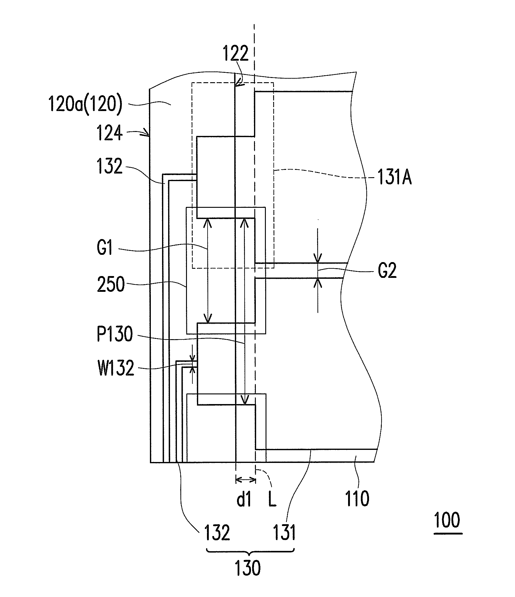
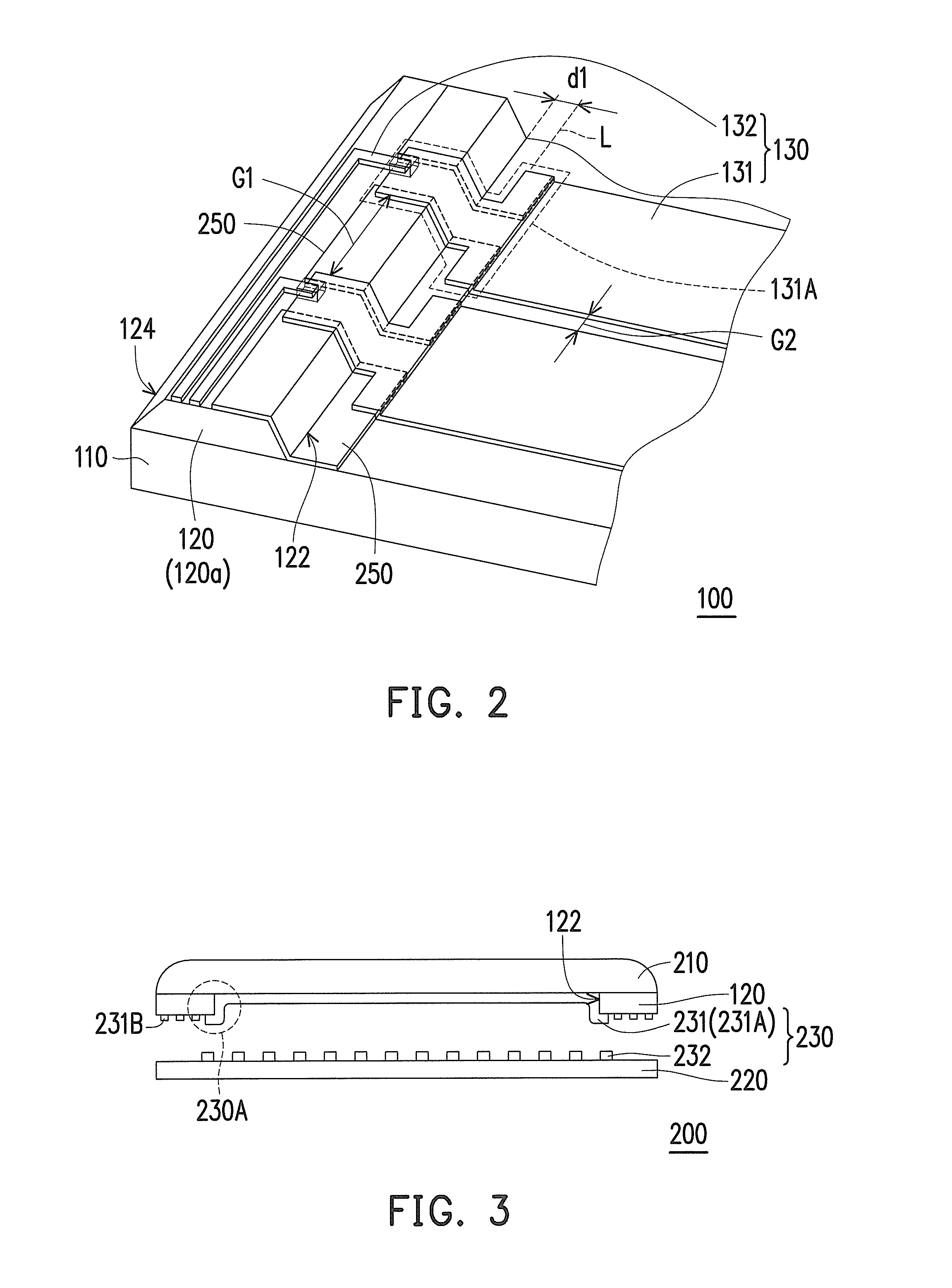
[0025]FIG. 1 is a partial schematic diagram illustrating a touch panel according to the invention, and FIG. 2 is a schematic perspective view of the touch panel in FIG. 1. Referring to FIG. 1 and FIG. 2, a touch panel 100 includes a substrate 110, a decoration layer 120 and a plurality of conductive elements 130. The substrate 110 may be a rigid transparent substrate, such as a glass substrate, or may be a flexible transparent substrate, such as a plastic substrate, but is not limited thereto. A material of the decoration layer 120 may include at least one of a ceramic, a diamond-like carbon, an organic material, an organic inorganic hybrid compound, or a mixture of an organic material and an inorganic material, but not limited thereto. For example, the decoration layer 120 can be photosensitive resin, such as photoresist, or non-photosensitive resin, such as ink. The conductive elements 130 are made of a conductive material, which includes a transparent conductive material, such as...

second embodiment

[0036]Structures of the conductive elements 230 and the decoration layer 120 in the above embodiment are only provided as example for the description purposes, and the invention is not limited thereto. For example, FIG. 4A and FIG. 4B are a schematic top view and a partial schematic top view illustrating a touch panel according to the invention. FIG. 5A is a schematic cross sectional view illustrating the touch panel in FIG. 4B along a profile line I-I′; and FIG. 5B is a schematic cross sectional view illustrating the touch panel in FIG. 4B along a profile line II-II′. Referring to FIG. 4A, FIG. 4B and FIG. 5A at the same time, a touch panel 300 includes a substrate 310, a decoration layer 320, a plurality of conductive elements 330, an insulating layer 350 and a protective layer 360. The decoration layer 320 is disposed on at least one side of the substrate 310. The conductive elements 330 construct a plurality of touch sensing units 331 and connecting wires 332. The touch sensing ...

third embodiment

[0045]When the touch panel 300 is fabricated with the components, such as the decoration layer 320 and the conductive elements 330, on the substrate 310 after the substrate 310 is cut into a predetermined size, the edge of the decoration layer 320 and the edge of the substrate 310 may be aligned with each other, but the invention is not limited thereto. For example, FIG. 6 a schematic cross sectional view illustrating a touch panel according to the invention. Referring to FIG. 6, a touch panel 400 is generally similar to the touch panel 300, and thus the same or the similar components in the two embodiments are to be represented with the same or similar element symbols. In the present embodiment, the touch panel 400 includes the substrate 310, a decoration layer 420, the conductive elements 330, the insulating layer 350, the protective layer 360, a strengthening layer 430 and a light shielding layer 440. The light shielding layer 440 includes a light resistant material, which may be...


PUM


Abstract

A touch panel including a substrate, a decoration layer, and conductive elements is provided. The decoration layer has an outer margin adjacent to an edge of the substrate and an inner margin opposite to the outer region. A reference line is away from the inner margin with a distance of at least 20 μm towards a direction away from the outer margin. At least one of the conductive elements includes a cross-interface portion which covers the decoration layer and a region of the substrate without the decoration layer. A first distance and a second distance between two adjacent cross-interface portions are provided in a region outward of the reference line to the outer margin of the decoration layer, and in a region inward of the reference line, respectively. The first distance is greater than the second distance. The conductive elements construct touch sensing units for forming a capacitance coupling.

Description

CROSS-REFERENCE TO RELATED APPLICATION[0001]This application claims the priority benefit of Taiwan application serial no. 102102028, filed on Jan. 18, 2013. The entirety of the above-mentioned patent application is hereby incorporated by reference herein and made a part of this specification.BACKGROUND[0002]1. Field of the Application[0003]The invention relates to a touch panel, and more particularly, to a touch panel disposed with a light resistant layer.[0004]2. Description of Related Art[0005]Input interfaces for many information products have been transformed from the traditional devices, such as keyboard or mouse, to touch devices. Therefore, the touch panel has been subjected to a wide range of applications. Generally, in order to transmit signals generated by an operation of a user using the touch panel, a plurality of wires are usually required and preferably disposed at a peripheral region of the touch panel. In order to avoid the wires be exposed on the outside of the touc...

Claims


Application Information

Patent Timeline
IPC IPC(8): G06F3/044
CPCG06F3/044G06F2203/04107G06F3/04164G06F3/0446G06F3/0443
Inventor LIN, YI-CHUNWU, MING-KUNGHWANG, CHIN-PEICHEN, KUO-HSINGCHEN, YU-TINGSU, CHEN-HAOLEE, YUN-BINSU, KUO-CHANGLI, YAN-LING
Owner WINTEK CORP
Why Eureka
Try Eureka