Method of manufacturing input device

a manufacturing method and input device technology, applied in the direction of optics, instruments, printed circuit aspects, etc., can solve the problems of short circuit and deterioration of the sensitivity of the input device b>101/b>, and achieve the effect of suppressing the occurrence of disconnection of the lead electrode, improving the environmental resistance of the input device, and suppressing the generation of blisters

Inactive Publication Date: 2014-08-14
ALPS ALPINE CO LTD
View PDF5 Cites 1 Cited by
  • Summary
  • Abstract
  • Description
  • Claims
  • Application Information

AI Technical Summary

Benefits of technology

[0013]The present invention provides an input device that can improve environmental resistance by suppressing the occurrence of the disconnection of lead electrodes, a short circuit, and the like and can prevent blisters from being generated between a surface member and an optical adhesive layer, and a method of manufacturing the input device.

Problems solved by technology

For this reason, since the exposed portions 132a of the lead electrodes are affected by humidity, temperature, and the like of external air, there is a concern that disconnection caused by corrosion, a short circuit caused by the attachment of foreign materials, and the like may occur.
However, since it is difficult to apply the sealing resin 161 while accurately controlling the thickness of the sealing resin 161, the sealing resin 161 is applied with a large thickness.
For this reason, there is a possibility that the sensitivity of a sensor of the input device 101 may deteriorate.

Method used


Image

  • Method of manufacturing input device
  • Method of manufacturing input device
  • Method of manufacturing input device

Examples


first embodiment

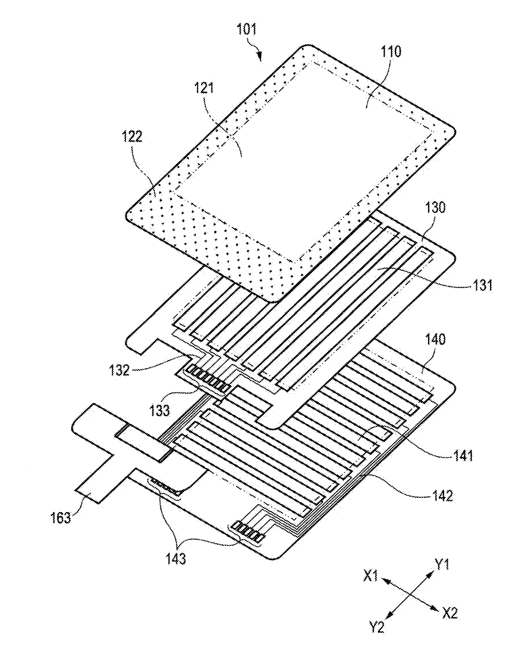
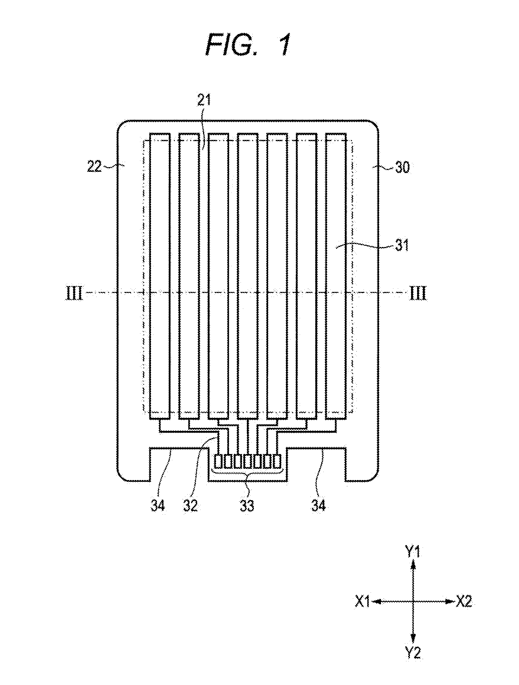
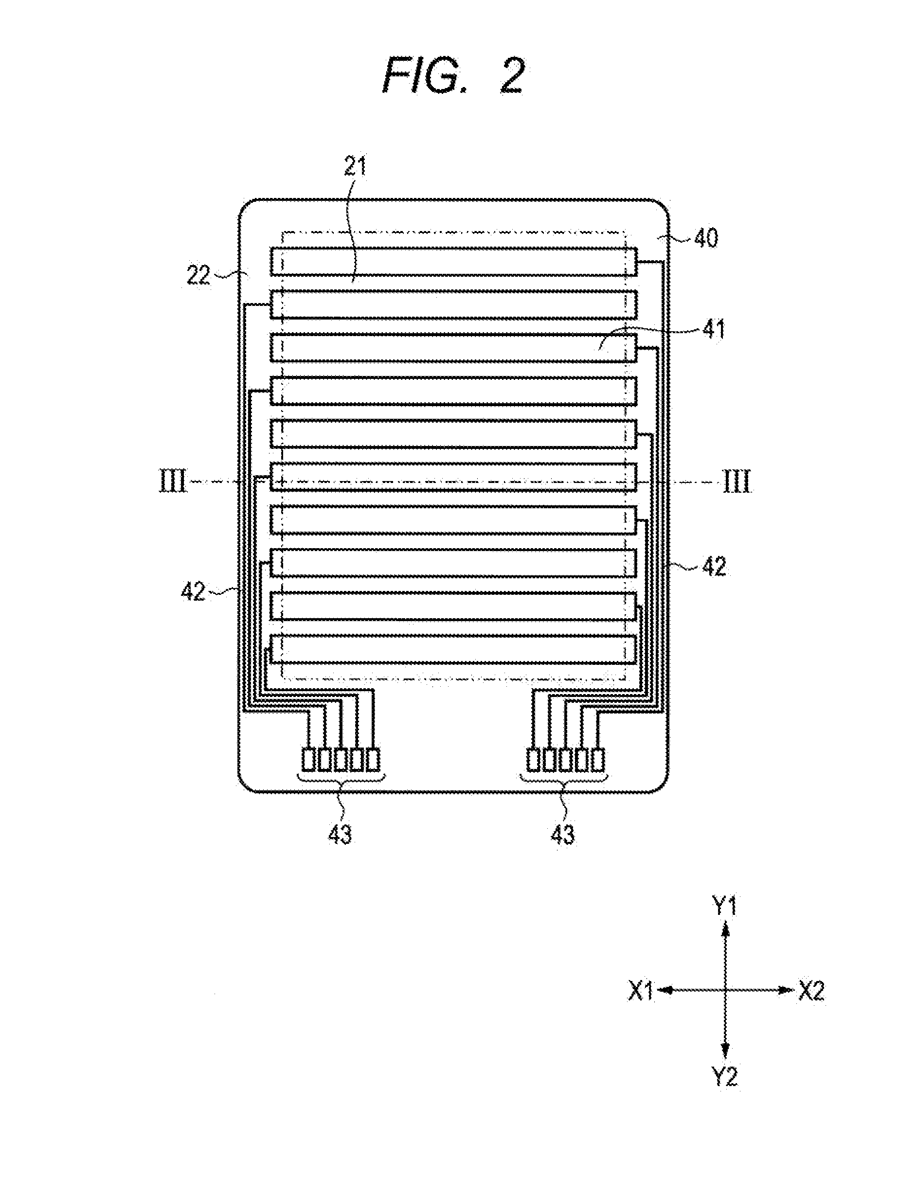
[0039]FIG. 1 is a plan view of a first transparent base 30 of an input device 1 according to a first embodiment. FIG. 2 is a plan view of a second transparent base 40 of the input device 1 according to the first embodiment. Further, FIG. 3 is a cross-sectional view of the input device 1, where the respective transparent bases and a surface member 10 are laminated and assembled, taken along a line III-III of FIGS. 1 and 2.

[0040]As shown in FIG. 1, a first transparent electrode layer 31, first lead electrodes 32, and first connection electrodes 33 are formed on one surface of the first transparent base 30. As shown in FIG. 1, the first transparent electrode layer 31 is formed of a plurality of strip-shaped bodies extending in a Y1-Y2 direction and the plurality of strip-shaped bodies are arranged parallel to each other at intervals in an X1-X2 direction.

[0041]The first transparent electrode layer 31 is formed in an input region 21 of the first transparent base 30, and a frame-like non...

second embodiment

[0069]FIG. 9 is a schematic plan view of the vicinity of a connecting portion of an input device 1 according to a second embodiment that is to be connected to an FPC 63. FIG. 10 is a schematic cross-sectional view of the input device 1 taken along a line X-X of FIG. 9. Meanwhile, the same components as the components of the first embodiment are denoted by the same reference numerals and the detailed description thereof will be omitted.

[0070]As in the first embodiment, in the input device 1 according to this embodiment, first and second transparent bases 30 and 40 and a surface member 10 are laminated with first and second optical adhesive layers 51 and 52 interposed therebetween. Further, a transparent electrode layer, lead electrodes, and connection electrodes are formed on each of the first and second transparent bases 30 and 40.

[0071]As shown in FIGS. 9 and 10, the first optical adhesive layer 51 and the FPC 63 are disposed on one surface of the first transparent base 30 with a p...


PUM

PropertyMeasurementUnit
thicknessaaaaaaaaaa
thicknessaaaaaaaaaa
thicknessaaaaaaaaaa

Abstract

A method of manufacturing an input device includes a step of bonding a translucent first optical adhesive layer to one surface of a first transparent base so that a part of first lead electrodes is exposed to the outside; a step of disposing a FPC so that a predetermined gap is formed between the FPC and the first optical adhesive layer in plan view, and electrically connecting the FPC to the first lead electrodes exposed to one surface of the first transparent base; a step of bonding a surface member, which forms an input surface, to the first transparent base with the first optical adhesive layer interposed therebetween; and a step of sealing the exposed lead electrodes by injecting a resin into a space between the first transparent base and the surface member facing each other.

Description

CLAIM OF PRIORITY[0001]This application is a Divisional of U.S. patent application Ser. No. 13 / 294,457 filed on Nov. 11, 2011, which claims benefit of Japanese Patent Application No. 2011-050942 filed on Mar. 9, 2011, both of which are hereby incorporated by reference.BACKGROUND OF THE INVENTION[0002]1. Field of the Invention[0003]The present invention relates to an input device and a method of manufacturing the input device, and more particularly, to an input device that can improve environmental resistance and a method of manufacturing the input device.[0004]2. Description of the Related Art[0005]Currently, a translucent input device is used as a display portion of an electronic device such as a mobile phone. An input device is disposed so as to overlap a display device such as liquid crystal, and a user can be in visual contact with an image, which is displayed on the display device, through the input device. Further, a user can input position information by touching an input reg...

Claims


Application Information

Patent Timeline
Patent Type & Authority Applications(United States)
IPC IPC(8): H01H11/06
CPCH01H11/06G06F2203/04103G06F3/0445Y10T29/49124Y10T29/49126G02F1/13452G06F3/041H05K3/321H05K2201/10128
Inventor HORINO, TAKENOBU
Owner ALPS ALPINE CO LTD
Why Eureka
Try Eureka