Three dimensional NAND device with semiconductor, metal or silicide floating gates and method of making thereof

Active Publication Date: 2014-08-14
SANDISK TECH LLC
View PDF7 Cites 122 Cited by
  • Summary
  • Abstract
  • Description
  • Claims
  • Application Information

AI Technical Summary

Benefits of technology

[0003]An embodiment relates to a method of making a monolithic three dimensional NAND string, which includes forming a stack of alternating layers of a first material and a second material, where the first material comprises an electrically insulating material and wherein the second material comprises a sacrificial material, etching the stack to form a front side opening in the stack, selectively forming a plurality of discrete semiconductor, metal or silicide charge storage regions on portions of the second material layers exposed in the front side opening, forming a tunnel dielectric layer over the charge storage regions in the front side opening, forming a semiconductor channel layer over the tunnel dielectric layer in the front side opening, etching the stack to form a back side opening in the stack, removing at least a portion of the second material layers through the back side opening to form back side recesses between the first material layers, forming a blocking dielectric in the back side recesses through the back side opening, and forming control gates over the blocking dielectric in the back side recesses through the back side opening.

Problems solved by technology

Furthermore, the active regions of the NAND string is formed by a relatively difficult and time consuming process involving repeated formation of sidewall spacers and etching of a portion of the substrate, which results in a roughly conical active region shape.

Method used


Image

  • Three dimensional NAND device with semiconductor, metal or silicide floating gates and method of making thereof
  • Three dimensional NAND device with semiconductor, metal or silicide floating gates and method of making thereof
  • Three dimensional NAND device with semiconductor, metal or silicide floating gates and method of making thereof

Examples


Embodiment Construction

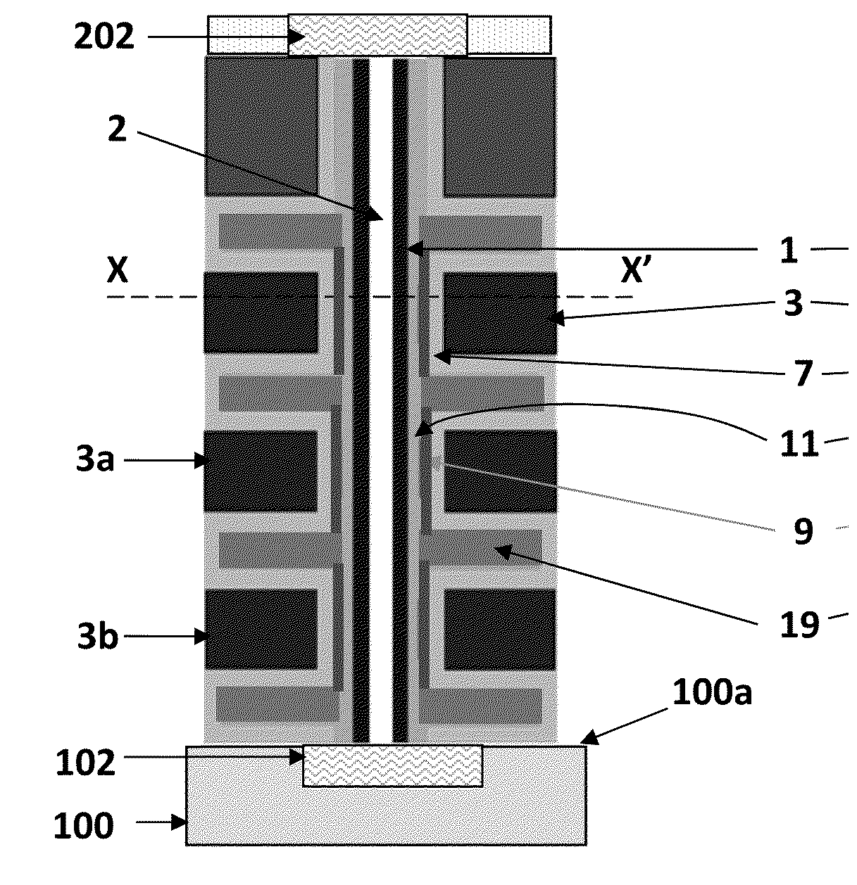
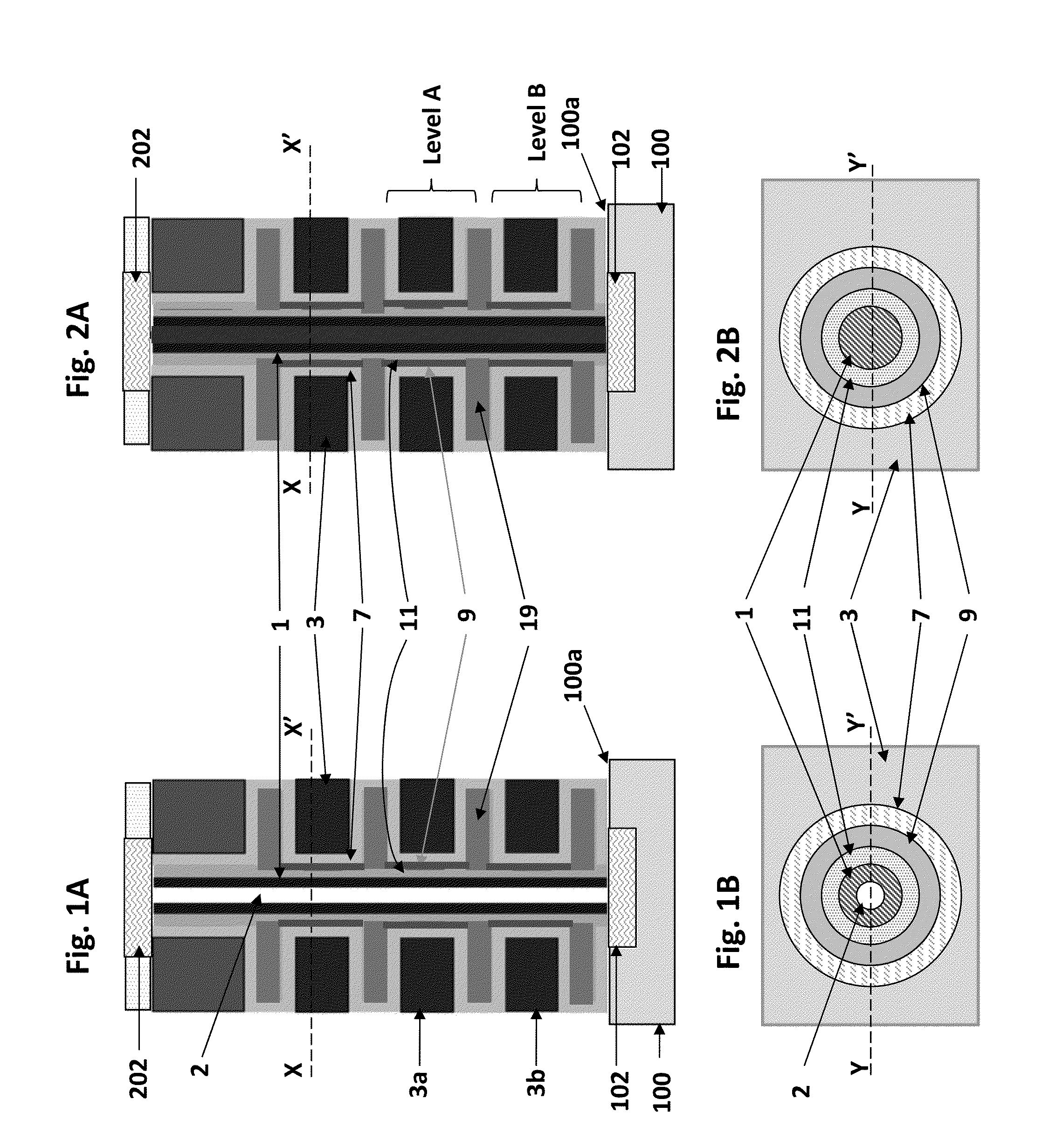
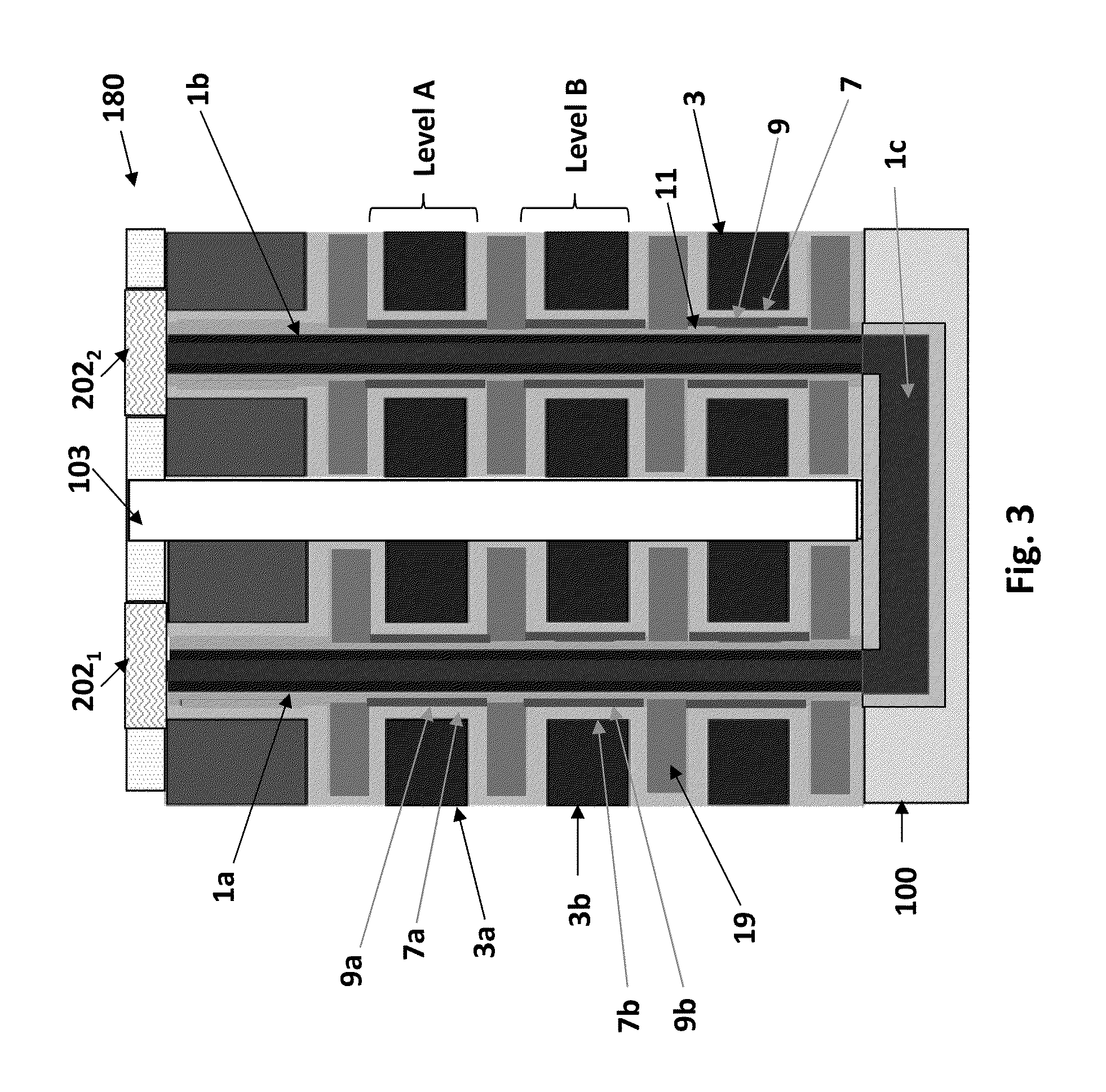
[0012]The embodiments of the invention provide a monolithic, three dimensional array of memory devices, such as an array of vertical NAND strings having selectively formed, discreet metal, semiconductor or silicide charge storage regions. The NAND strings are vertically oriented, such that at least one memory cell is located over another memory cell. The array allows vertical scaling of NAND devices to provide a higher density of memory cells per unit area of silicon or other semiconductor material.

[0013]A monolithic three dimensional memory array is one in which multiple memory levels are formed above a single substrate, such as a semiconductor wafer, with no intervening substrates. The term “monolithic” means that layers of each level of the array are directly deposited on the layers of each underlying level of the array. In contrast, two dimensional arrays may be formed separately and then packaged together to form a non-monolithic memory device. For example, non-monolithic stack...


PUM

PropertyMeasurementUnit
thickaaaaaaaaaa
depthaaaaaaaaaa
pressureaaaaaaaaaa

Abstract

A method of making a monolithic three dimensional NAND string includes forming a stack of alternating layers of a first material and a second material, etching the stack to form a front side opening in the stack, selectively forming a plurality of discrete semiconductor, metal or silicide charge storage regions on portions of the second material layers exposed in the front side opening, forming a tunnel dielectric layer and semiconductor channel layer in the front side opening, etching the stack to form a back side opening in the stack, removing at least a portion of the second material layers through the back side opening to form back side recesses between the first material layers, forming a blocking dielectric in the back side recesses through the back side opening, and forming control gates over the blocking dielectric in the back side recesses through the back side opening.

Description

FIELD[0001]The present invention relates generally to the field of semiconductor devices and specifically to three dimensional vertical NAND strings and other three dimensional devices and methods of making thereof.BACKGROUND[0002]Three dimensional vertical NAND strings are disclosed in an article by T. Endoh, et. al., titled “Novel Ultra High Density Memory With A Stacked-Surrounding Gate Transistor (S-SGT) Structured Cell”, IEDM Proc. (2001) 33-36. However, this NAND string provides only one bit per cell. Furthermore, the active regions of the NAND string is formed by a relatively difficult and time consuming process involving repeated formation of sidewall spacers and etching of a portion of the substrate, which results in a roughly conical active region shape.SUMMARY[0003]An embodiment relates to a method of making a monolithic three dimensional NAND string, which includes forming a stack of alternating layers of a first material and a second material, where the first material c...

Claims


Application Information

Patent Timeline
Patent Type & Authority Applications(United States)
IPC IPC(8): H01L27/088H01L29/66
CPCH01L29/66825H01L27/088H01L29/7889H01L29/40114H01L29/40117H10B41/27H01L21/8221H10B99/00
Inventor MAKALA, RAGHUVEER S.ALSMEIER, JOHANN
Owner SANDISK TECH LLC
Why Eureka
Try Eureka