Waveguide-coupled vertical cavity laser

a vertical cavity laser and waveguide technology, applied in lasers, lasers, laser output parameters control, etc., can solve the problems of low wall-plug efficiency of conventional wdm laser sources, difficult to produce suitable low-cost wdm optical sources, and a large obstacle to the implementation of wdm silicon-photonic links

Active Publication Date: 2014-08-14
ORACLE INT CORP
View PDF10 Cites 5 Cited by
  • Summary
  • Abstract
  • Description
  • Claims
  • Application Information

AI Technical Summary

Benefits of technology

[0009]Note that a given mirror, which can be the first mirror or the second mirror, may include a stack, out of the plane of the semiconductor layer, of alternating materials having a first index of refrac

Problems solved by technology

However, producing a suitable low-cost WDM optical source remains a challenge and poses an obstacle to implementing WDM silicon-photonic links.

Method used


Image

  • Waveguide-coupled vertical cavity laser
  • Waveguide-coupled vertical cavity laser
  • Waveguide-coupled vertical cavity laser

Examples


Embodiment Construction

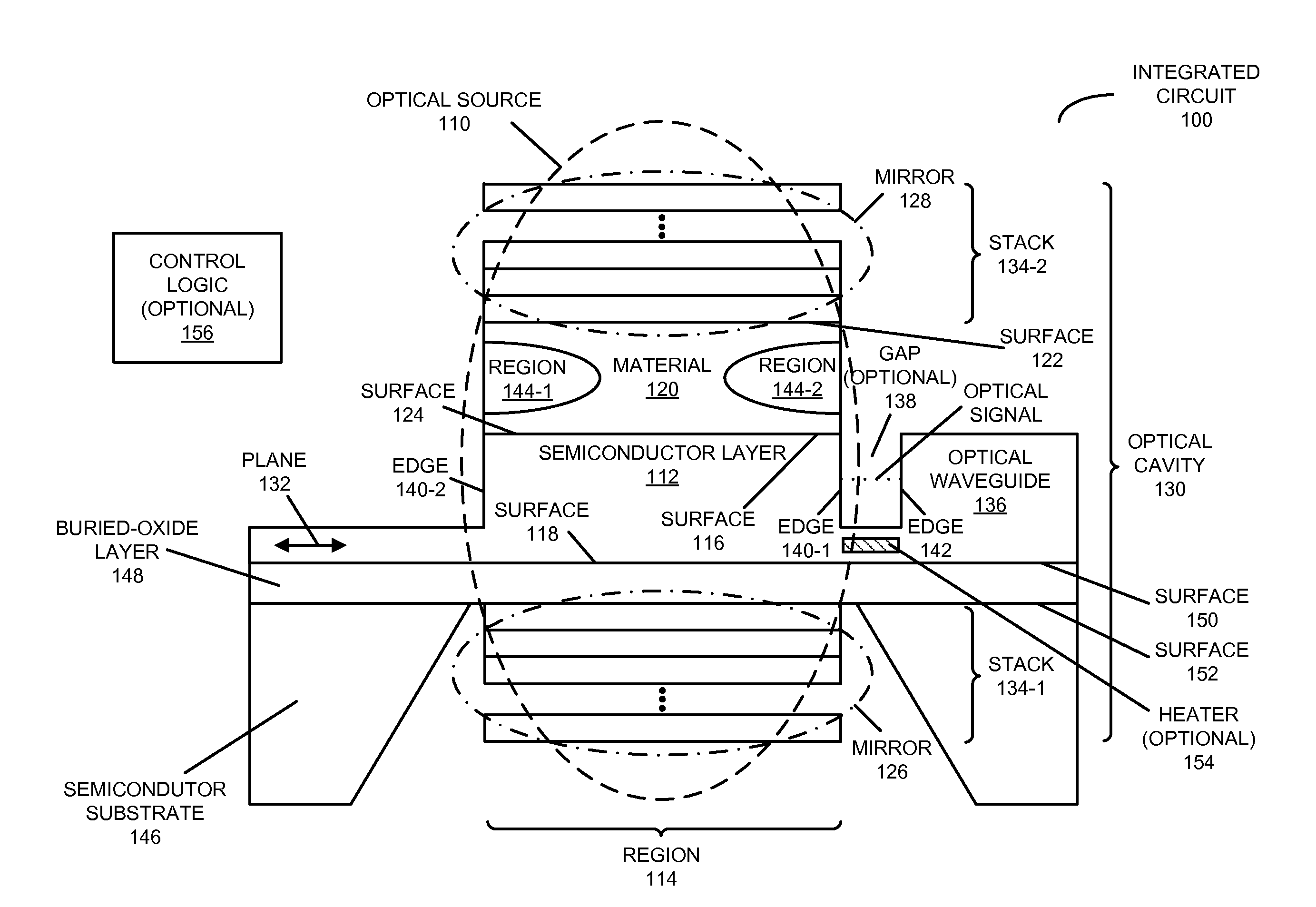
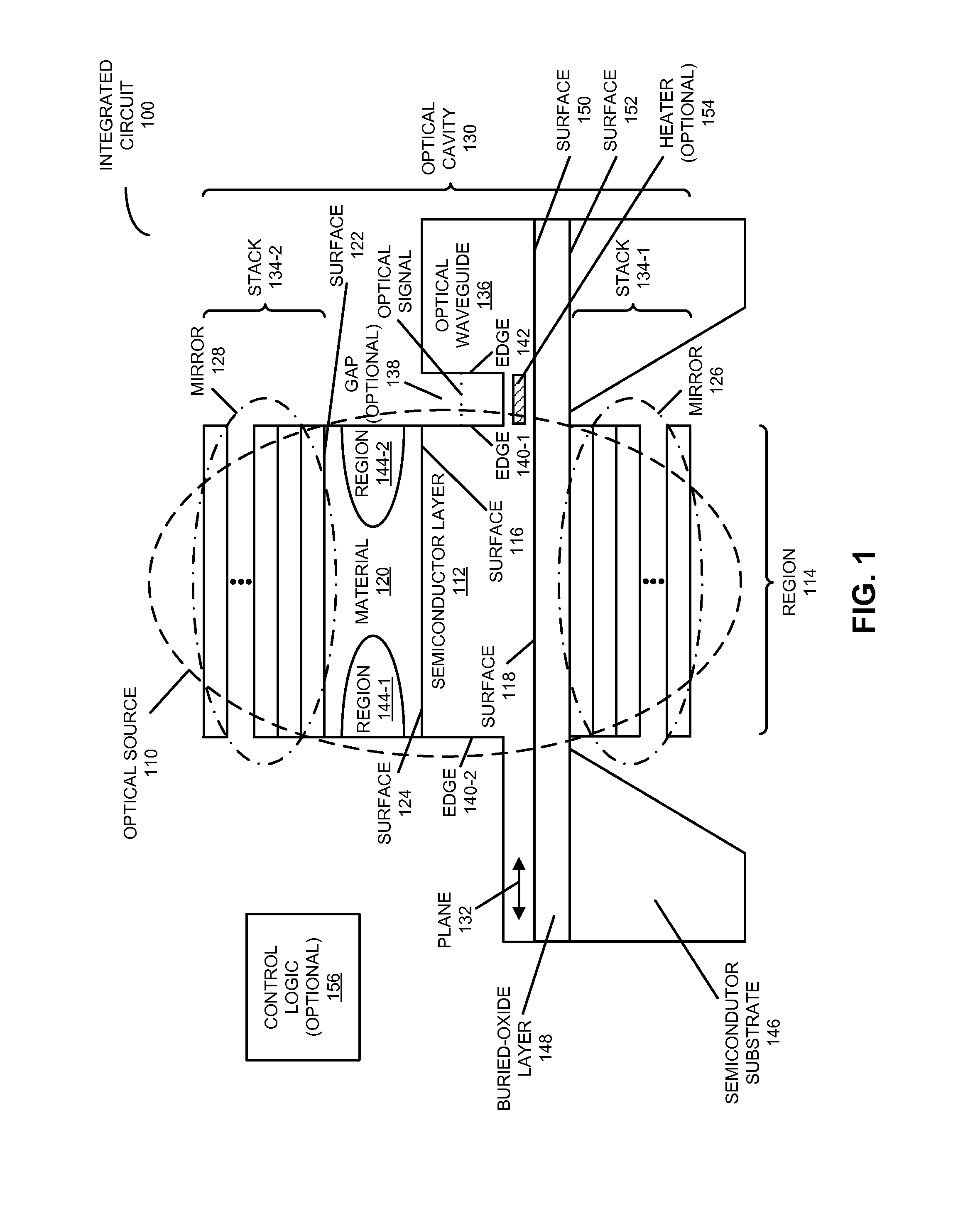
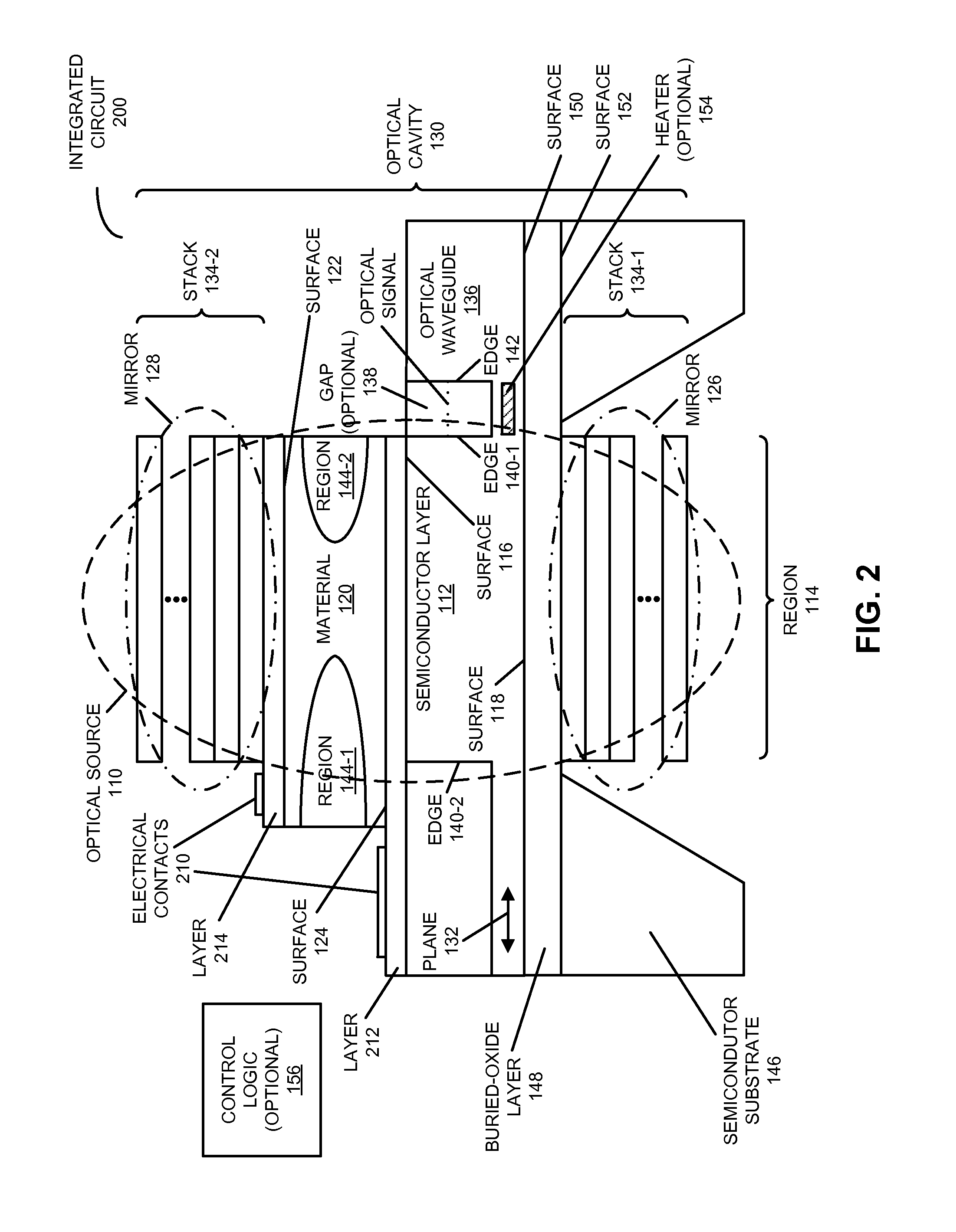
[0024]Embodiments of an integrated circuit, a system that includes the integrated circuit, and a technique for providing an optical signal are described. The integrated circuit includes an optical source that provides the optical signal to an optical waveguide. In particular, the optical source may be implemented by fusion-bonding a III-V semiconductor to a semiconductor layer in the integrated circuit. In conjunction with surrounding mirrors (at least one of which is other than a distributed Bragg reflector and, more generally, a reflector that includes multiple layers with alternating indices of refraction), this structure may provide a cavity with suitable optical gain at a wavelength in the optical signal along a vertical direction that is perpendicular to a plane of the semiconductor layer. For example, the optical source may include a vertical-cavity surface-emitting laser (VCSEL). Moreover, the optical waveguide, defined in the semiconductor layer, may be separated from the o...


PUM


Abstract

An integrated circuit includes an optical source that provides an optical signal to an optical waveguide. In particular, the optical source may be implemented by fusion-bonding a III-V semiconductor to a semiconductor layer in the integrated circuit. In conjunction with surrounding mirrors (at least one of which is other than a distributed Bragg reflector), this structure may provide a cavity with suitable optical gain at a wavelength in the optical signal along a vertical direction that is perpendicular to a plane of the semiconductor layer. For example, the optical source may include a vertical-cavity surface-emitting laser (VCSEL). Moreover, the optical waveguide, defined in the semiconductor layer, may be separated from the optical source by a horizontal gap in the plane of the semiconductor layer. During operation of the optical source, the optical signal may be optically coupled across the gap from the optical source to the optical waveguide.

Description

GOVERNMENT LICENSE RIGHTS[0001]This invention was made with Government support under Agreement No. HR0011-08-9-0001 awarded by DARPA. The Government has certain rights in the invention.BACKGROUND[0002]1. Field[0003]The present disclosure relates to techniques for communicating optical signals. More specifically, the present disclosure relates to an integrated circuit that includes an optical source.[0004]2. Related Art[0005]Silicon photonics is a promising technology that can provide large communication bandwidth, low latency and low power consumption for inter-chip and intra-chip connections. In the last few years, significant progress has been made in developing low-cost components for use in inter-chip and intra-chip silicon-photonic connections, including: high-bandwidth efficient silicon modulators, low-loss optical waveguides, wavelength-division-multiplexing (WDM) components, and high-speed CMOS optical-waveguide photodetectors. However, producing a suitable low-cost WDM opti...

Claims


Application Information

Patent Timeline
IPC IPC(8): H01S5/20H01S5/06
CPCH01S5/06H01S5/20H01S5/026H01S5/021H01S5/0215H01S5/0218H01S5/0612H01S5/06804H01S5/1032H01S5/18308H01S5/18341H01S5/18358H01S5/18361H01S5/2045H01S5/3013
Inventor KRISHNAMOORTHY, ASHOK V.CUNNINGHAM, JOHN E.ZHENG, XUEZHE
Owner ORACLE INT CORP
Why Eureka
Try Eureka