Surface-emitting laser device and surface-emitting laser array including same

a laser array and laser device technology, applied in semiconductor lasers, laser cooling arrangements, laser details, etc., can solve the problems of poor temperature characteristics, inferior output of surface-emitting laser devices in the 780 nm band, and inability to obtain high outpu

Active Publication Date: 2010-04-06
RICOH KK
View PDF58 Cites 40 Cited by
  • Summary
  • Abstract
  • Description
  • Claims
  • Application Information

AI Technical Summary

Benefits of technology

[0053]Embodiments of the present invention may solve or reduce one or more of the above-described problems.
[0054]According to one embodiment of the present invention, there is provided a surface-emitting laser device in which one or more of the above-described problems may be solved or reduced.

Problems solved by technology

However, since the volume of the active layer is small in surface-emitting laser devices, surface-emitting laser devices are lower in light output than edge-emitting lasers, so as to be often required to increase output.
In particular, as the wavelength becomes shorter, confinement of carriers in the active layer becomes poorer, thus causing problems such as inability to obtain high output and poor temperature characteristics.
However, an output of 7 mW has been reported in the 850 nm and 980 nm bands, showing that the surface-emitting laser device of the 780 nm band is inferior in output.
This decreases light emission efficiency and reliability.
However, there is a problem in that surface-emitting laser devices of short oscillation wavelengths are low in output.
However, in semiconductor lasers, Al is regarded as a cause of device degradation.
Since AlGaAs-system materials inherently contain a cause of degradation, it is difficult to realize a highly reliable device with AlGaAs-system materials.
However, the band discontinuity of the valence bands of these materials is relatively large, which may cause an increase in device resistance.
At this point, it is highly possible that a defect is introduced at their interface to cause various problems.
However, since the AlGaInP-system material is inferior in thermal conductivity to the AlGaAs-system material, the temperature of the active layer is likely to increase during oscillation so as to degrade many characteristics.
In the case of increasing image recording speed by this method, however, many problems such as development of a light source for high laser output or a highly sensitive photosensitive body, reinforcement of a housing that supports high-speed main and sub scanning, and development of a position control method at the time of high-speed scanning, thus necessitating expenditure of large amounts of money and time.
However, with a configuration using an edge-emitting semiconductor laser as described in Patent Document 5, the number of beams is about four or at most eight for structural and cost reasons, so that it is impossible to support high-speed image outputting, which is expected to make progress in the future.
However, conventional surface-emitting laser devices have the problem of low output because carrier confinement is insufficient and heat generated in the active layer is less likely to be transferred outside.

Method used


Image

  • Surface-emitting laser device and surface-emitting laser array including same
  • Surface-emitting laser device and surface-emitting laser array including same
  • Surface-emitting laser device and surface-emitting laser array including same

Examples


first embodiment

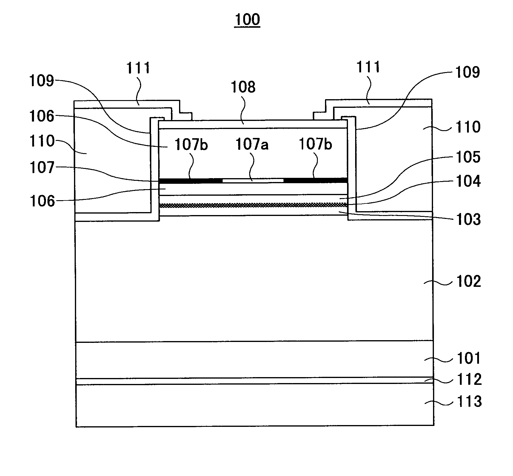
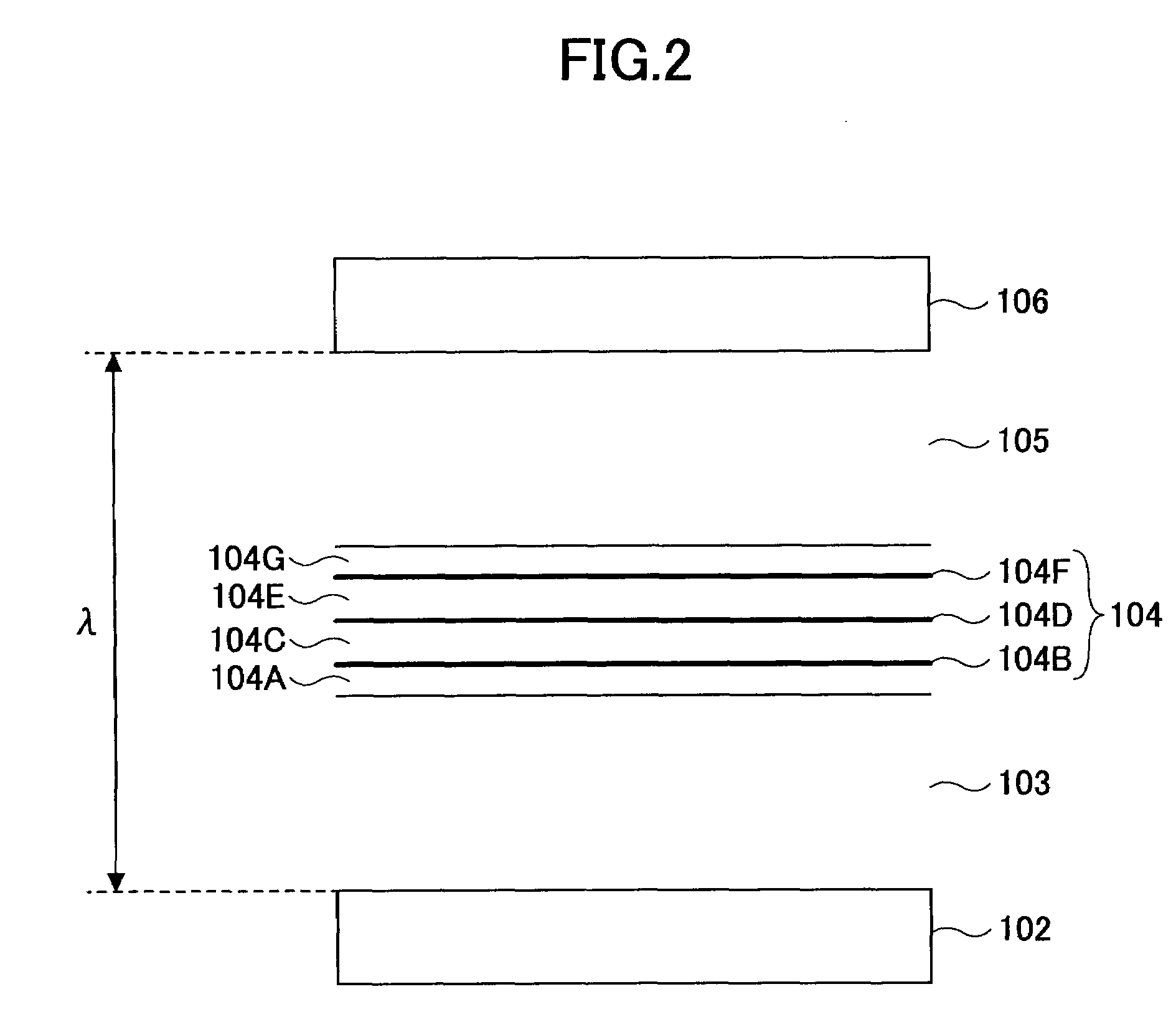
[0146]FIG. 1 is a schematic cross-sectional view of a surface-emitting laser device 100 according to a first embodiment of the present invention. Referring to FIG. 1, the surface-emitting laser device 100 includes a substrate 101, reflective layers 102 and 106, cavity spacer layers 103 and 105, an active layer 104, a selectively oxidized layer 107, a contact layer 108, a SiO2 layer 109, insulating resin 110, a p-side electrode 111, and an n-side electrode 112. The surface-emitting laser device 100 is a 780 nm band surface-emitting laser device.

[0147]The substrate 101 is formed of (100) n-type gallium arsenide (n-GaAs) whose surface orientation is inclined at an inclination angle of 15 degrees to the direction of a (111)A surface. The reflective layer 102 is formed of 35.5 periods of [n-Al0.9Ga0.1As / n-Al0.3Ga0.7As], letting a pair of n-Al0.9Ga0.1As / n-Al0.3Ga0.7As be one period, and is formed on a principal plane of the substrate 101. Letting the oscillation wavelength of the surface-...

second embodiment

[0217]FIG. 7 is a schematic cross-sectional view of a surface-emitting laser device 100A according to a second embodiment of the present invention. Referring to FIG. 7, the surface-emitting laser device 100A is the same as the surface-emitting laser device 100 shown in FIG. 1 except that the cavity spacer layer 103 of the surface-emitting laser device 100 is replaced with a cavity spacer layer 103A.

[0218]The cavity spacer layer 103A is formed of Al0.4Ga0.6As. In the surface-emitting laser device 100A, since the cavity spacer layer 105 is formed of (Al0.7Ga0.3)0.5In0.5P, the cavity spacer layer 103A has a greater thermal conductivity than the cavity spacer layer 105. (See the curved lines k1 and k2 of FIG. 6). Thus, the surface-emitting laser device 100A has the two cavity spacer layers 103A and 105 formed of semiconductor materials asymmetrical with respect to the active layer 104, and the cavity spacer layer 103A disposed on the substrate 101 side of the active layer 104 is formed ...

third embodiment

[0221]FIG. 8 is a schematic cross-sectional view of a surface-emitting laser device 100B according to a third embodiment of the present invention. Referring to FIG. 8, the surface-emitting laser device 100B is the same as the surface-emitting laser device 100 shown in FIG. 1 except that the cavity spacer layer 103 of the surface-emitting laser device 100 is replaced with a cavity spacer layer 103B.

[0222]FIG. 9 is a cross-sectional view of part of the two reflective layers 102 and 106, the two cavity spacer layers 103B and 105, and the active layer 104 shown in FIG. 8. Referring to FIG. 9, the cavity spacer layer 103B includes spacer layers 1031 and 1032. The spacer layer 1031 is formed in contact with the reflective layer 102 and the spacer layer 1032 is formed in contact with the spacer layer 1031 and the active layer 104.

[0223]The spacer layer 1031 is formed of lattice-matching Ga0.5In0.5P, and the spacer layer 1032 is formed of (Al0.7Ga0.3)0.5In0.5P.

[0224]According to the surface...


PUM


Abstract

A surface-emitting laser device is disclosed that includes a substrate connected to a heat sink; a first reflective layer formed of a semiconductor distributed Bragg reflector on the substrate; a first cavity spacer layer formed in contact with the first reflective layer; an active layer formed in contact with the first cavity spacer layer; a second cavity spacer layer formed in contact with the active layer; and a second reflective layer formed of a semiconductor distributed Bragg reflector in contact with the second cavity spacer layer. The first cavity spacer layer includes a semiconductor material having a thermal conductivity greater than the thermal conductivity of a semiconductor material forming the second cavity spacer layer.

Description

CROSS-REFERENCE TO RELATED APPLICATION[0001]The present application is a continuation-in-part application of PCT International Application No. PCT / JP2007 / 052298, filed on Feb. 2, 2007, which claims priority to Japanese Priority Patent Applications No. 2006-027466, filed on Feb. 3, 2006, No. 2006-057535, filed on Mar. 3, 2006, and No. 2006-250384, filed on Sep. 15, 2006.[0002]The present application is also based on Japanese Priority Patent Application No. 2007-046247, filed on Feb. 26, 2007.[0003]The entire contents of the foregoing applications are hereby incorporated by reference.BACKGROUND OF THE INVENTION[0004]1. Field of the Invention[0005]The present invention relates to a surface-emitting laser device, a surface-emitting laser array including the same, an image forming apparatus including the surface-emitting laser array, an optical pickup unit including the surface-emitting laser device or the surface-emitting laser array, an optical transmitter module including the surface-...

Claims


Application Information

Patent Timeline
Patent Type & Authority Patents(United States)
IPC IPC(8): H01S5/00
CPCB82Y20/00H01S5/18311H01S5/02461H01S5/3436H01S5/3403H01S5/3434H01S5/18358
Inventor SATO, SHUNICHIHARA, KEIJIKUTANI, NAOTO
Owner RICOH KK
Why Eureka
Try Eureka