Light-emitting diode having chemical compound based reflective structure

a light-emitting diode and chemical compound technology, applied in the field of reflection structure, can solve the problems of poor difficult manufacturing, extra expense and labor consumption in the industry, etc., to reduce light escape, enhance the overall brightness of the light-emitting diode, and eliminate undeired light escape

Inactive Publication Date: 2005-05-19
ITE COMPOUND SEMICON CORP
View PDF4 Cites 42 Cited by
  • Summary
  • Abstract
  • Description
  • Claims
  • Application Information

AI Technical Summary

Benefits of technology

[0006] Thus, a primary object of the present invention is to provide a light emitting diode comprising a stack of reflective layers made of chemical compounds and having different reflection angle for effectively reflecting light having different incident angles thereby substantially eliminating undesired escape of light and enhancing overall brightness of the light emitting diode.
[0007] To achieve the above object, in accordance with one aspect of the present invention, a light-emitting diode light emitting diode comprises a plurality of reflective layers stacked on each other to form a reflection structure, each reflective layer comprising a distributed Bragg reflector; a substrate formed on a top surface of the stack of reflective layers; an N type semiconductor layer formed on the substrate; a light emitting layer formed on the N type semiconductor layer; and a P type semiconductor layer formed on the light emitting layer. The stack of reflective layers is formed under the substrate to receive and reflect light from the light emitting diode at different incident angles so as to reduce light

Problems solved by technology

However, undesired escape of light is still severe in this conventional structure, consequently leading to poor overall brightness of the light emitting diode.
Fu

Method used


Image

  • Light-emitting diode having chemical compound based reflective structure
  • Light-emitting diode having chemical compound based reflective structure
  • Light-emitting diode having chemical compound based reflective structure

Examples


Embodiment Construction

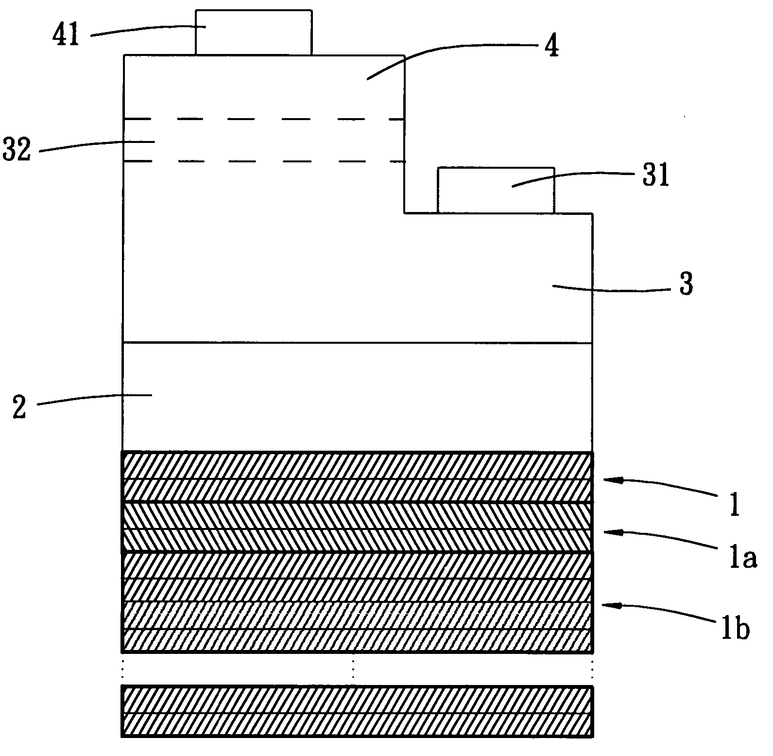
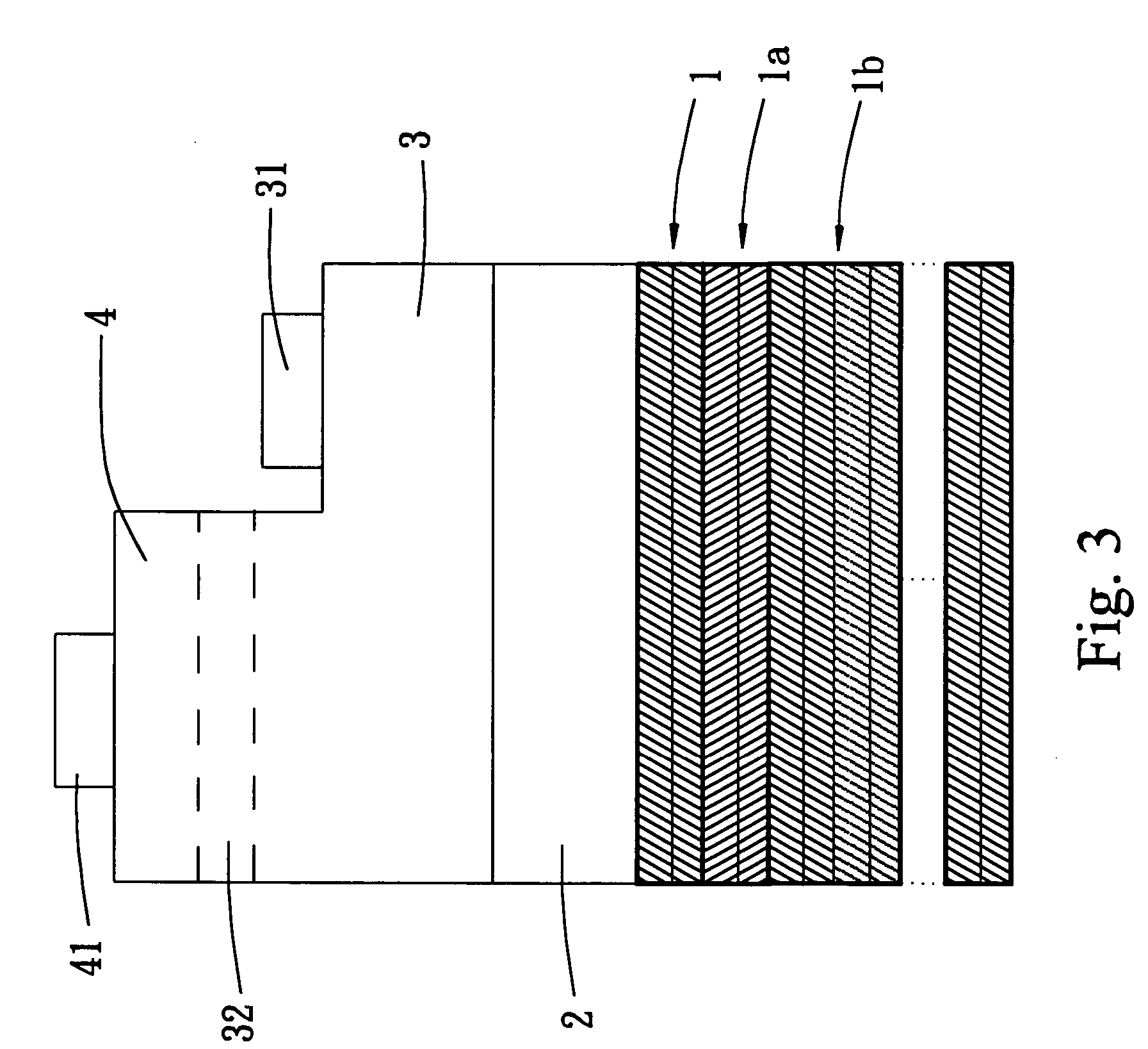
[0020] With reference to the drawings and in particular to FIG. 1, a light emitting diode (LED) constructed in accordance with the present invention comprises two reflective layers 1, 1a stacked over each other to form a reflection structure for the LED, a substrate 2, a light emitting layer 32, a N type semiconductor layer 3 and a P type semiconductor layer 4 stacked over each other in sequence. The reflective layers 1, 1a are sequentially deposited on an undersurface of the substrate 2 before the LED die is sliced and the reflective layers 1, 1a function to reflect light coming from the light emitting layer 32 and having different incident angles with respect to the substrate 2. Consequently, undesired escape of light from the LED can be alleviated and the brightness of the LED is enhanced.

[0021] In accordance with the present invention, the reflective layers 1, 1a comprise distributed Bragg reflector (DBR) and form a reflection structure together. The reflective layers 1, 1a are...


PUM


Abstract

A light-emitting diode (LED) includes a plurality of reflective layers stacked over each other and each comprising a distributed Bragg reflector, a substrate, an N type semiconductor formed on the substrate, a light emitting layer formed on the N type semiconductor layer and a P type semiconductor formed on the light emitting layer. The stack of the reflective layers is formed under the substrate or the stack is formed between the substrate and the N type semiconductor layer. The reflective layers receive and reflect light incident at different angles thereby alleviating escape of light from the light emitting diode and enhancing overall brightness of the light emitting diode.

Description

FIELD OF THE INVENTION [0001] The present invention generally relates to the filed of light-emitting diodes (LEDs), and in particular to an LED having reflection structure comprising a plurality of reflective layers of chemical compounds stacked over each other whereby light traveling toward the reflection structure at different incident angles are substantially reflected by the reflective layers so as to eliminate undesired escape of light from the LED and to enhance the overall brightness of the LED for better use in all kinds of display boards, lighting of large space, lighting for display of articles, lighting appliances and advertisement lighting boards. BACKGROUND OF THE INVENTION[0002] As shown in FIG. 6 of the attached drawings, a conventional light emitting diode (LED) is comprised of a transparent substrate 5, an N type semiconductor layer 6, a light emitting layer 62 and a P type semiconductor layer 7. The N type semiconductor layer 6 is formed on the transparent substrat...

Claims


Application Information

Patent Timeline
IPC IPC(8): H01L33/46
CPCH01L33/46
Inventor CHENG, WEI-TAIYEH, JUI-HUNG
Owner ITE COMPOUND SEMICON CORP
Why Eureka
Try Eureka