

Cover element and housing device for use of the cover element
- Summary
- Abstract
- Description
- Claims
- Application Information
AI Technical Summary
Benefits of technology
Problems solved by technology
Method used
Image

Examples
first embodiment
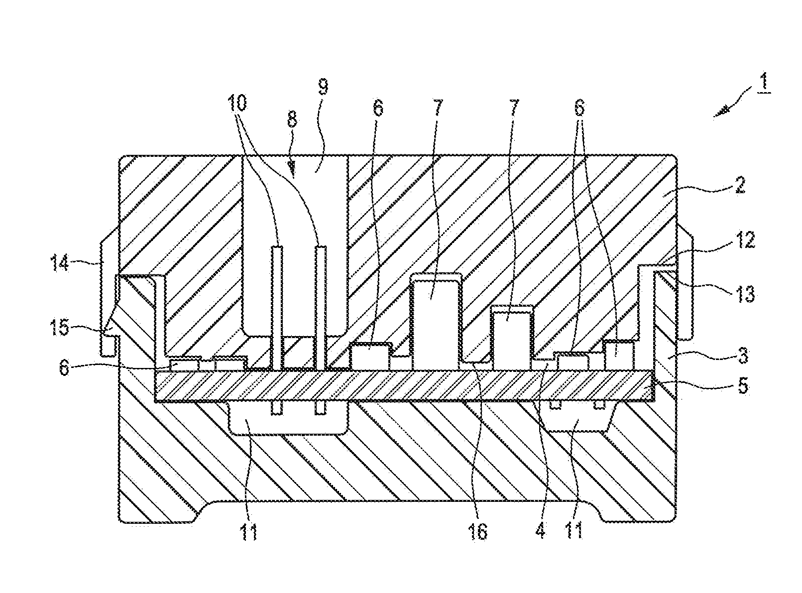
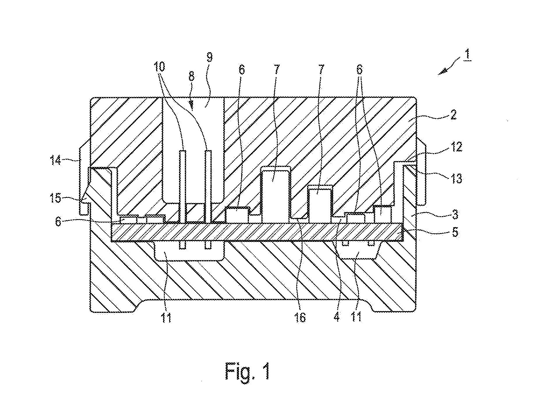
[0027]Referring to FIG. 1 a first embodiment of the present invention is described hereinafter.
[0028]FIG. 1 shows a housing device 1 in which a cover element 2 according to the invention is used. Besides the cover element 2, the housing device 1 includes a housing lower portion 3 which is so designed that the cover element 2 and the housing lower portion 3 can be connected together to form the housing device 1. The housing lower portion 3 is referred to hereinafter for simplicity as the lower portion 3.
[0029]Formed in the housing device 1 between the cover element 2 and the lower portion 3 is an internal space 4 in which parts to be disposed and protected by means of the housing device 1, like for example a printed circuit board 5 having a plurality of electric and electronic components and mechanical elements, are disposed. The present invention in connection with the cover element 2 is not limited to the arrangement of the printed circuit board 5 with further components. For the s...
second embodiment
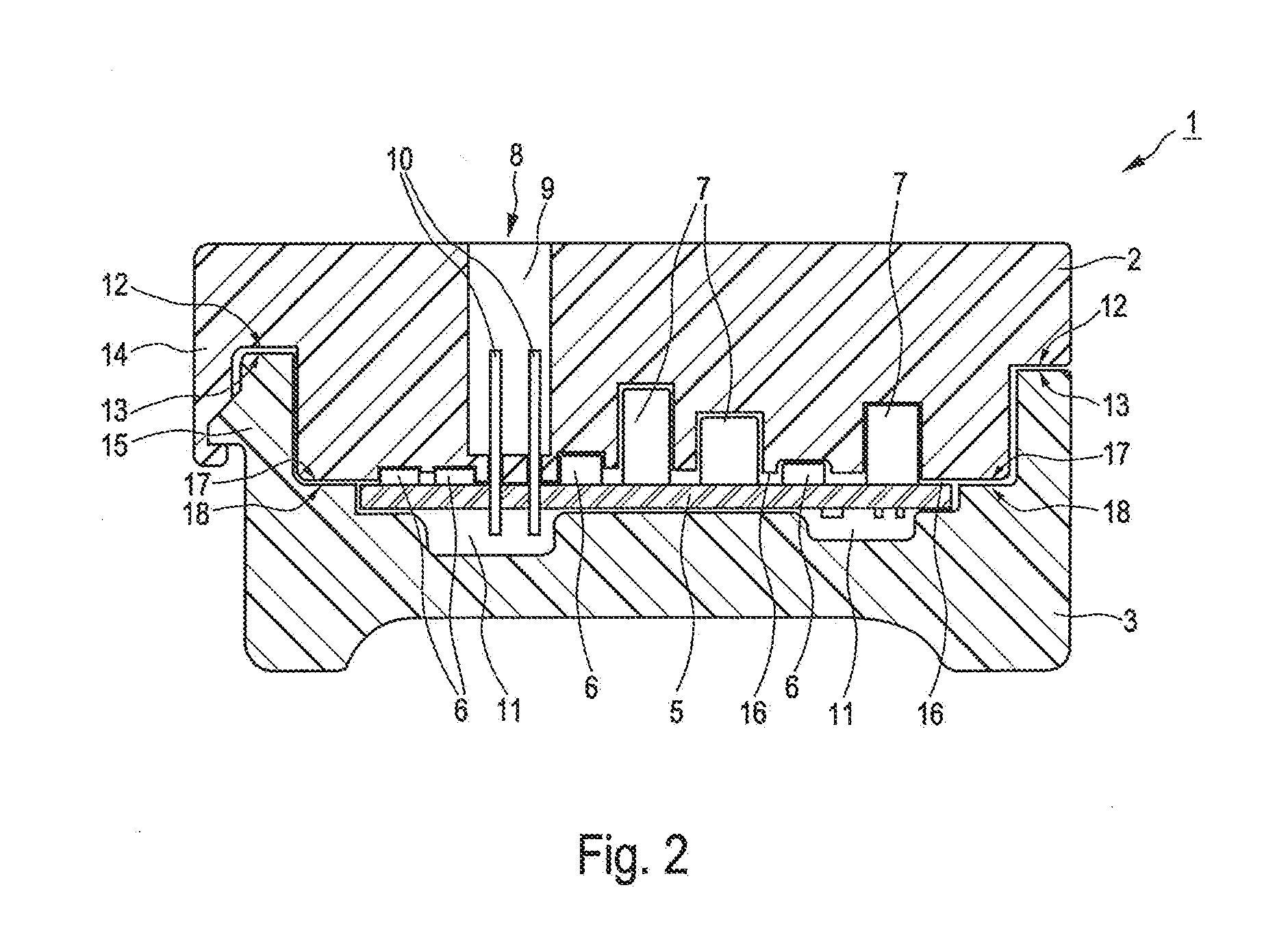
[0050]With reference to FIG. 2 a second embodiment of the present invention is described hereinafter. Similar or identical components or constituent parts are identified in the description of the second embodiment by the same references as in the first embodiment.
[0051]FIG. 2 shows a similar arrangement of the cover element 2 as shown in FIG. 1, the housing device 1 comprising the lower portion 3 and the cover element 2. The cover element 2 and the lower portion 3 can be connected together. For that purpose there can be fixing elements 14 and 15 and a latching connection can be made.
[0052]In the same manner as in the first embodiment, the second embodiment provides that the contour of the lower surface 16 of the cover element 2 approximately follows the contour of the inside surface of the printed circuit board 5 in conjunction with components 6 and 7 of differing size, shape and arrangement on the printed circuit board 5. Likewise there can be at least one plug region 8 with an ope...
PUM
 Abstract
Description
Claims
Application Information