
Organic light-emitting display device and method of fabricating the same

a technology of organic light-emitting display device and substrate, which is applied in the direction of semiconductor devices, electrical devices, chemistry apparatus and processes, etc., can solve the problems of cracks in the adhesive layer in the corner regions, and moisture entering the cracks through cracks to prevent moistur

Active Publication Date: 2014-08-21
LG DISPLAY CO LTD
View PDF8 Cites 1 Cited by
  • Summary
  • Abstract
  • Description
  • Claims
  • Application Information

AI Technical Summary

Benefits of technology

The patent describes an organic light-emitting display device that prevents cracks in the adhesive layer at the corner regions. This is achieved by designing rounded corner regions that allow for controlled formation of cracks and prevent moisture from reaching the active area of the device. Additionally, the patent suggests adding metallic connections to reduce signal delay in larger display devices. These connections are made through an auxiliary electrode and an auxiliary metallic pattern. Overall, the patent aims to improve the reliability and performance of organic light-emitting display devices.

Problems solved by technology

This may cause the adhesive layer to be more concentrated to the corner regions.
As a result, cracks may form in the adhesive layer in the corner regions when the adhesive layer is hardened.
Moisture may penetrate through the cracks into the organic light-emitting display device.
This will negatively affect the quality of the organic light-emitting display device, for example by shortening the lifespan of the device.

Method used


Image

  • Organic light-emitting display device and method of fabricating the same
  • Organic light-emitting display device and method of fabricating the same
  • Organic light-emitting display device and method of fabricating the same

Examples


Embodiment Construction

[0021]Description will now be given in detail of the exemplary embodiments, with reference to the accompanying drawings. For the sake of brief description with reference to the drawings, the same or equivalent components will be provided with the same reference numbers, and description thereof will not be repeated.

[0022]The organic light-emitting display device controls the formation of cracks in the adhesive layer by rounding the corner regions of the adhesive layer. Rounding the corner regions prevents the formation of large cracks in the adhesive layer that would otherwise allow moisture to reach the active area of the display device.

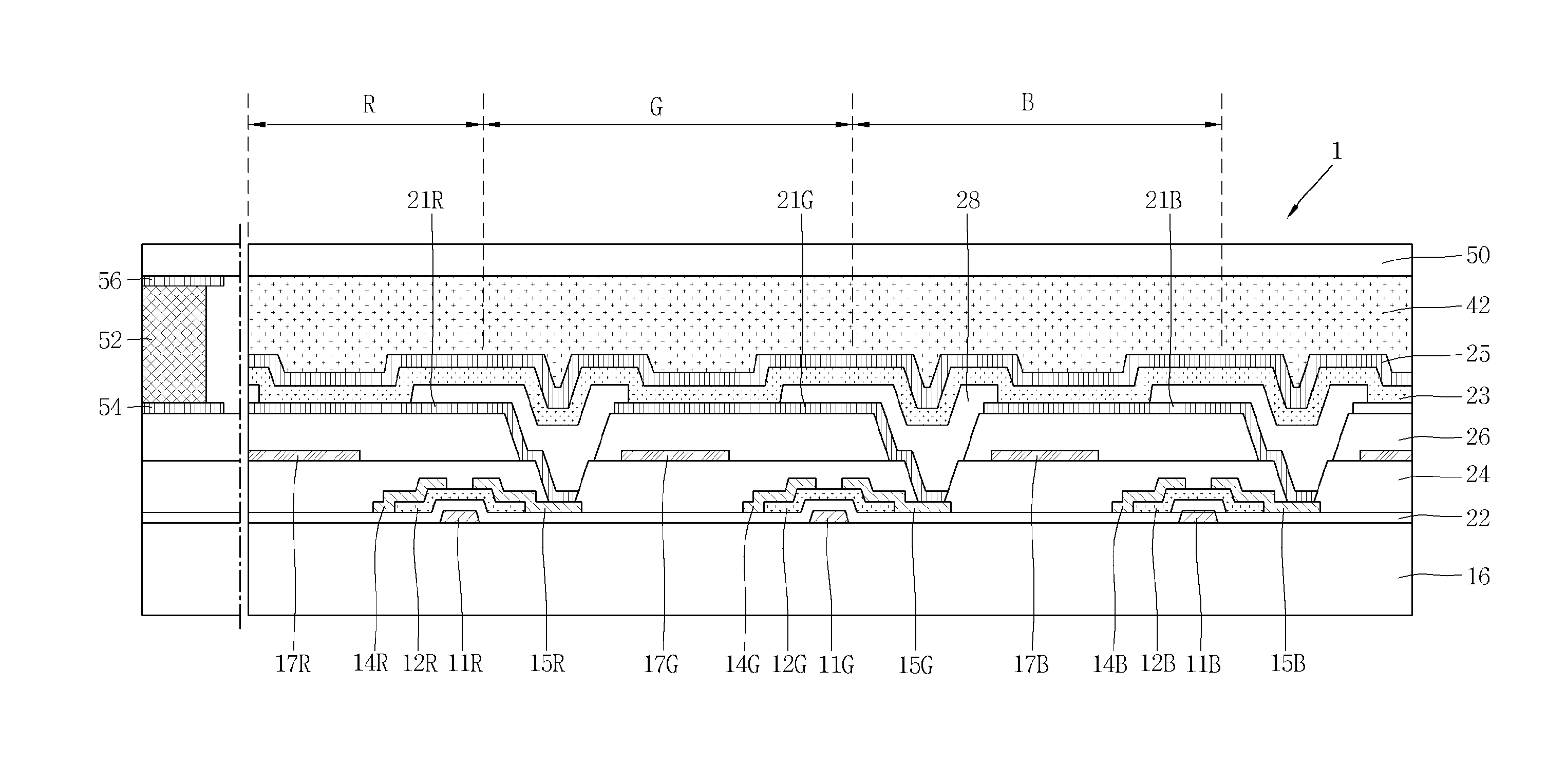
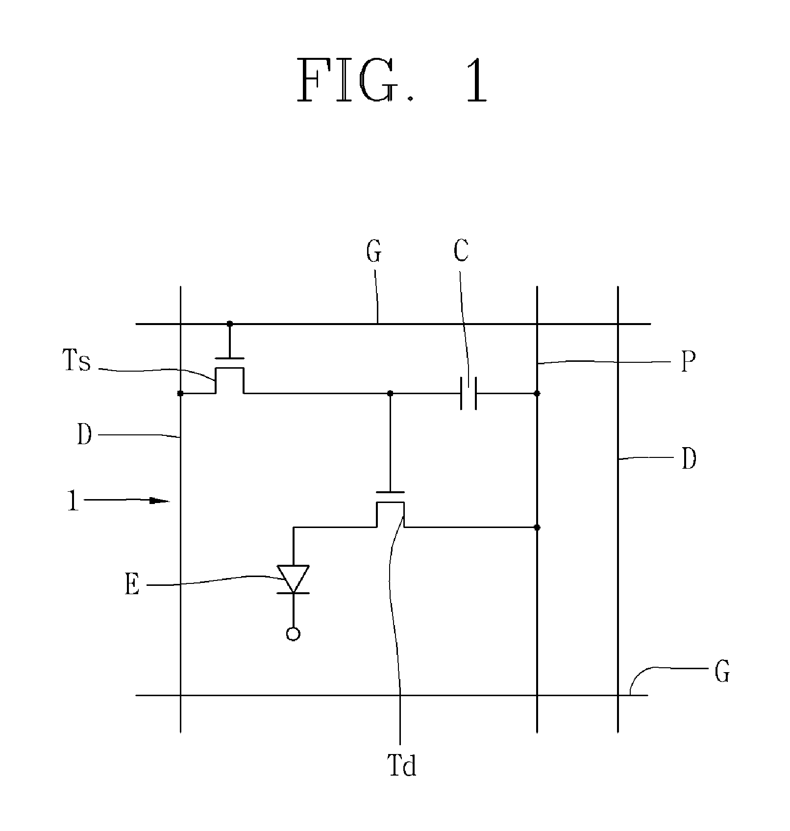
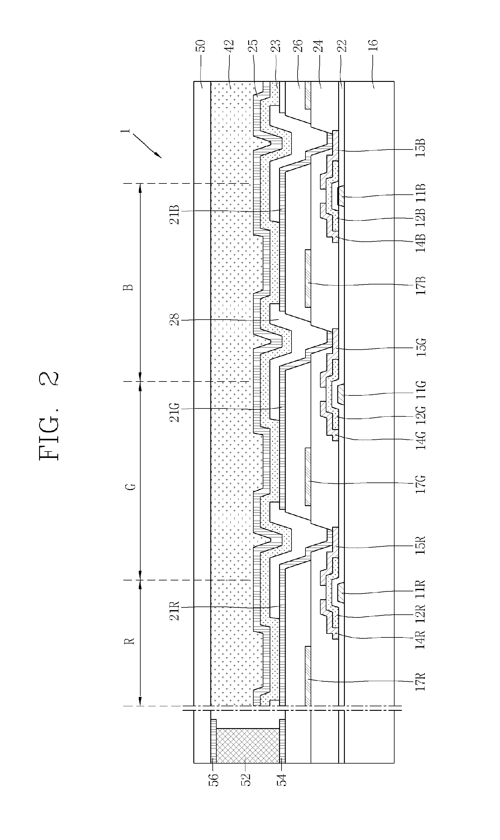
[0023]FIG. 1 is a view showing an equivalent circuit of an organic light-emitting display device according to the present disclosure. As shown in FIG. 1, the organic light-emitting display device 1 comprises a plurality of pixels defined by gate lines (G) and data lines (D) crossing each other in horizontal and vertical directions. In each pixel, a p...


PUM


Abstract

Disclosed is an organic light-emitting display device capable of preventing the occurrence of cracks at corner regions of an adhesive layer. The organic light-emitting display device includes a first substrate including a plurality of pixels and a second substrate. A thin film transistor (TFT) located at each pixel of the first substrate. A pixel electrode is also located at each pixel. An organic light-emitting unit that emits light is coupled to each pixel electrode. A common electrode is electrically coupled to each organic light-emitting unit. An adhesive layer is coupled to the common electrode. The adhesive layer attaches the first and second substrates. The corner regions of the adhesive layer are rounded in order to control the creation of cracks in the adhesive layer and thereby prevent moisture from entering the active area of the device.

Description

CROSS REFERENCE TO RELATED APPLICATION[0001]This application is a division of co-pending U.S. Application Ser. No. 13 / 454,755, filed Apr. 24, 2012, which claims the benefit of Korean Patent Application No. 10-2011-0094808, filed on Sep. 20, 2011, all of which are incorporated by reference herein in their entirety.BACKGROUND OF THE DISCLOSURE[0002]1. Field of the Disclosure[0003]The present disclosure relates to an organic light-emitting display device, and particularly, to designs of adhesive layers of an organic light-emitting display device to control the introduction of cracks in the adhesive layer.[0004]2. Discussion of the Related Art[0005]Organic light-emitting display devices have been noted as being one potential type of next generation display device due to the advantages inherent in their design, for example their high light-emitting efficiency, ease of constructing a large area device, simplified manufacturing processes, their ability to produce blue light, and their inhe...

Claims


Application Information

Patent Timeline
Patent Type & Authority Applications(United States)
IPC IPC(8): H01L51/56
CPCH01L2227/323H01L51/56H10K59/35H10K59/12H10K71/40H10K59/8722B32B37/12H10K59/122H10K71/00H10K50/8426H10K59/1201
Inventor KANG, JIN-GOOSHIN, JOO-HWAN
Owner LG DISPLAY CO LTD
Learn More