

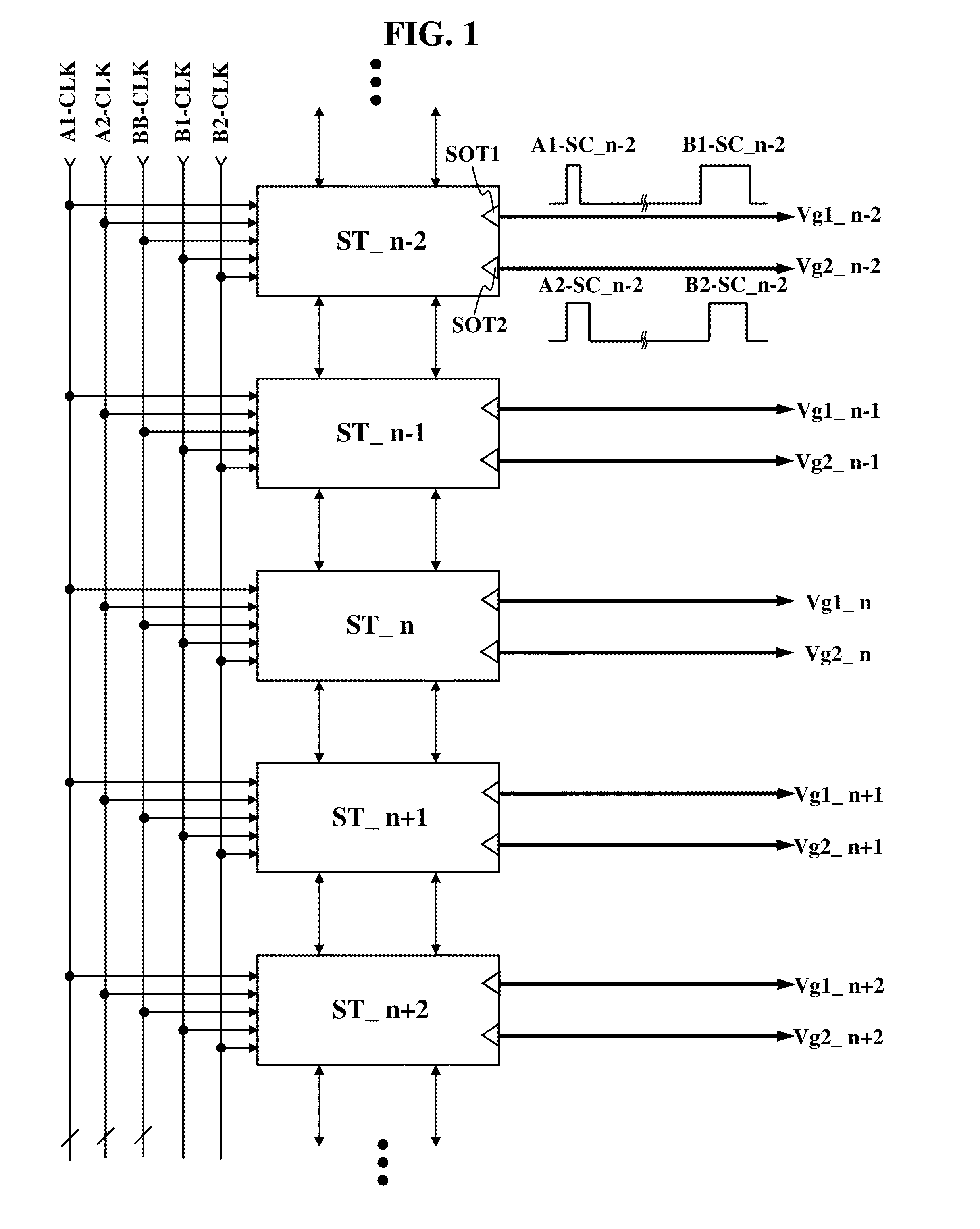
Shift register
a technology of shift register and shift register, which is applied in the field of shift register, can solve the problems of increasing the size of the display device, and achieve the effect of stable output and relatively small size of the scan output switching devi
- Summary
- Abstract
- Description
- Claims
- Application Information
AI Technical Summary
Benefits of technology
Problems solved by technology
Method used
Image

Examples
sixth embodiment
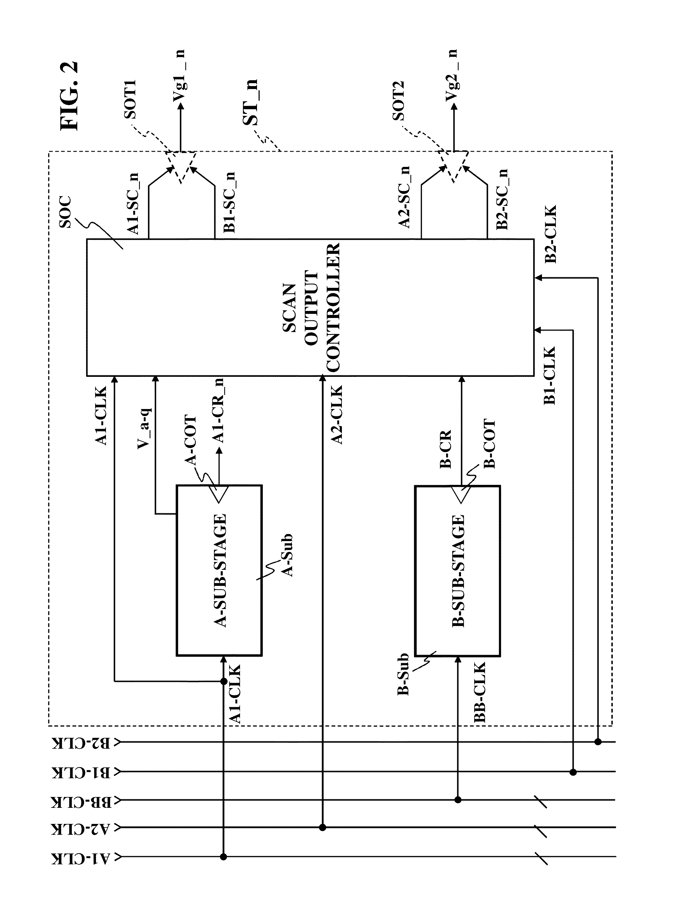
of Scan Output Controller SOC
[0167]FIG. 14 is a circuit diagram of a sixth embodiment of the scan output controller SOC according to the present invention.
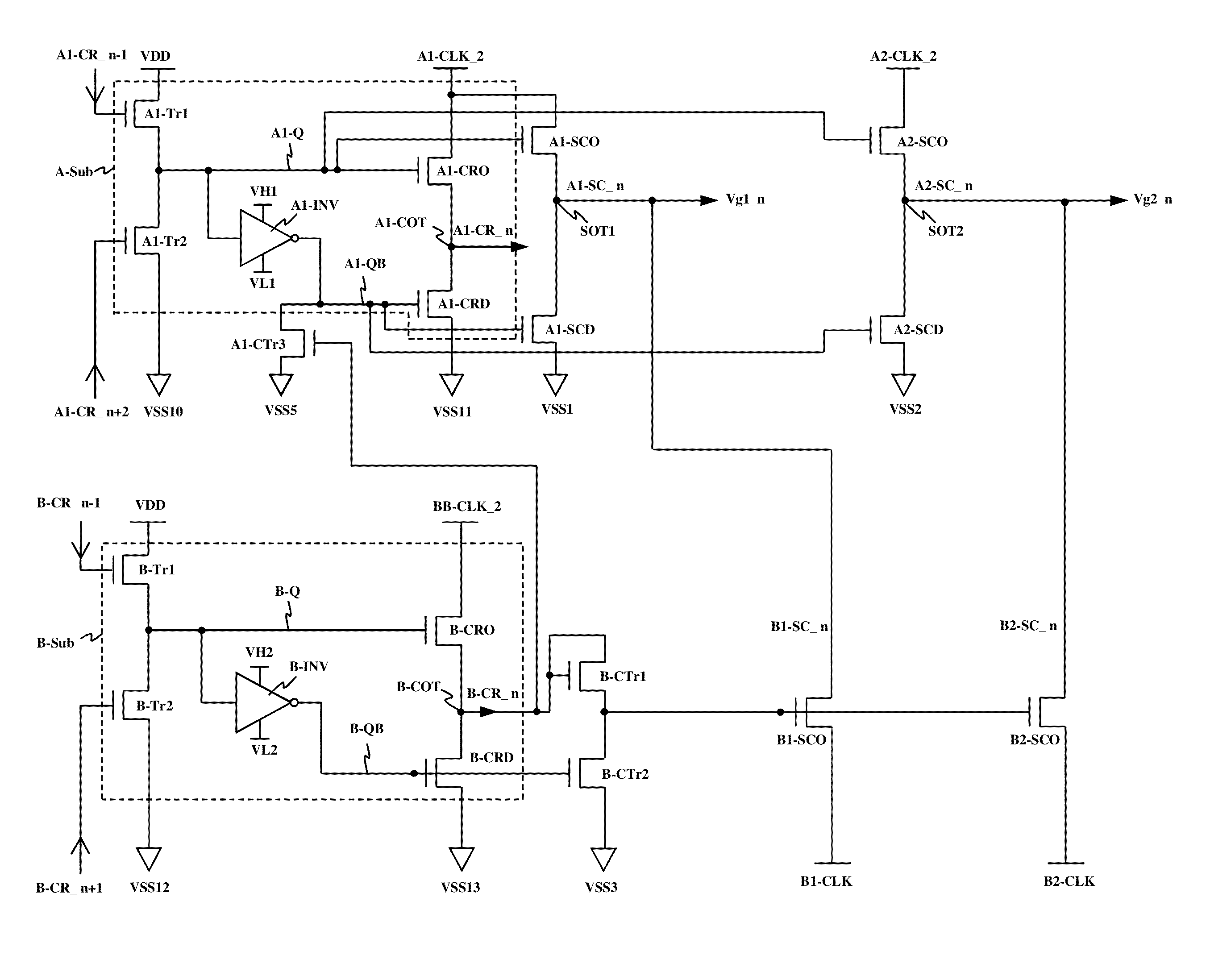
[0168]The scan output controller SOC according to the sixth embodiment includes an A1-scan output switching device A1-SCO, an A2-scan output switching device A2-SCO, an A1-scan discharge switching device A1-SCD, and an A2-scan discharge switching device A2-SCD, as shown in FIG. 14.
[0169]The A1-scan output switching device A1-SCO and A2-scan output switching device A2-SCO in the sixth embodiment are the same as those in the first embodiment, stated above, respectively, and a description thereof will thus be replaced by the above description of the first embodiment.
[0170]The A1-scan discharge switching device A1-SCD in the sixth embodiment is controlled by a voltage at an A-reset node A-QB and is connected between the first scan output terminal SOT1 and a first discharging voltage line which transfers a first discharging voltage VSS...
seventh embodiment
of Scan Output Controller SOC
[0174]FIG. 15 is a circuit diagram of a seventh embodiment of the scan output controller SOC according to the present invention.
[0175]The scan output controller SOC according to the seventh embodiment includes a B1-scan output switching device B1-SCO and a B2-scan output switching device B2-SCO, as shown in FIG. 15.
[0176]The B1-scan output switching device B1-SCO in the seventh embodiment is controlled by a B-carry pulse B-CR_n and is connected between a B1-clock transfer line which transfers a B1-clock pulse B1-CLK and a first scan output terminal SOT 1. That is, the B1-scan output switching device B1-SCO is turned on or off in response to the B-carry pulse B-CR_n, and interconnects the B1-clock transfer line and the first scan output terminal SOT1 when turned on.
[0177]The B2-scan output switching device B2-SCO in the seventh embodiment is controlled by the B-carry pulse B-CR_n and is connected between a B2-clock transfer line which transfers a B2-clock...
eighth embodiment
of Scan Output Controller SOC
[0178]FIG. 16 is a circuit diagram of an eighth embodiment of the scan output controller SOC according to the present invention.
[0179]The scan output controller SOC according to the eighth embodiment includes a first B-control switching device B-CTr1, a B1-scan output switching device B1-SCO, a B2-scan output switching device B2-SCO, and a second B-control switching device B-CTr2, as shown in FIG. 16.
[0180]The first B-control switching device B-CTr1 in the eighth embodiment is controlled by an external switching control signal Vc and is connected between a B-carry output terminal B-COT and a B-node B-n. That is, the first B-control switching device B-CTr1 is turned on or off in response to the switching control signal Vc, and interconnects the B-carry output terminal B-COT and the B-node B-n when turned on.
[0181]The B1-scan output switching device B1-SCO in the eighth embodiment is controlled by a voltage at the B-node B-n and is connected between a B1-c...
PUM
 Abstract
Description
Claims
Application Information