Solid-state imaging device

a solid-state imaging and single-panel technology, applied in the direction of semiconductor devices, radio-controlled devices, electrical devices, etc., can solve the problems of low color reproducibility, deterioration of luminance and color reproducibility, and difficulty in determining the reproducibility of luminance and color, so as to achieve the effect of increasing resolution

Inactive Publication Date: 2014-09-25
FUJIFILM CORP
View PDF16 Cites 6 Cited by
  • Summary
  • Abstract
  • Description
  • Claims
  • Application Information

AI Technical Summary

Benefits of technology

[0026]According to the present invention, the pixel pairs, each of which is composed of left and right phase difference pixels, are arrayed in the light receiving area. One color filter is assigned to each pixel pair. The fundamental array pattern is composed of the N types of color filters arranged into a rectangular matrix of a predetermined pattern along the two slanting directions orthogonal to each other. This fundamental array pattern is repeatedly arranged in the horizontal direction and the vertical direction, to compose the color filter array. In the color filter array, the first filter, whi

Problems solved by technology

In this case, the reproducibility of luminance and color by a high-frequency signal contained in object light becomes a problem.
More specifically, a fold-back (aliasing) occurs in the high-frequency signal beyond a reproducible range of each color due to a color pattern of the color filter array, and deteriorates the reproducibility of luminance and color.
Thus, the reproducibility of color is low and may cause a false color.
However, the use of the optical low-pass filter degrades the resolution, and therefore improvement in the color pattern of the color filter array is attempted.
However, this color pattern is ineffective at improving

Method used


Image

  • Solid-state imaging device
  • Solid-state imaging device
  • Solid-state imaging device

Examples


Embodiment Construction

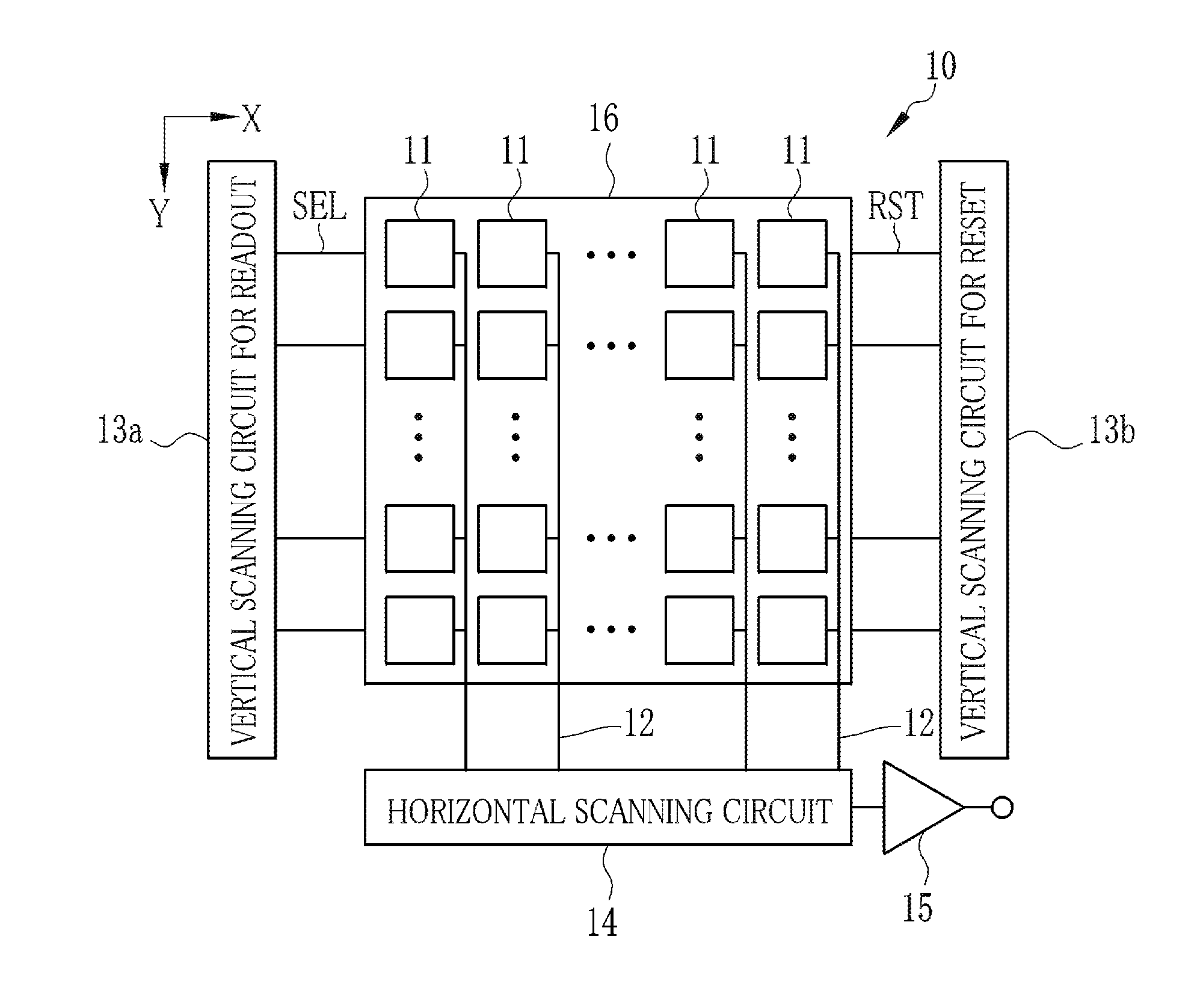
[0037]As shown in FIG. 1, a solid-state imaging device 10, being a CMOS image sensor, is provided with a plurality of pixels 11, vertical signal lines 12, a vertical scanning circuit 13a for readout, a vertical scanning circuit 13b for reset, a horizontal scanning circuit 14, a driving circuit (not shown) for driving each of the vertical scanning circuits 13a and 13b and the horizontal scanning circuit 14, an output circuit 15, and the like.

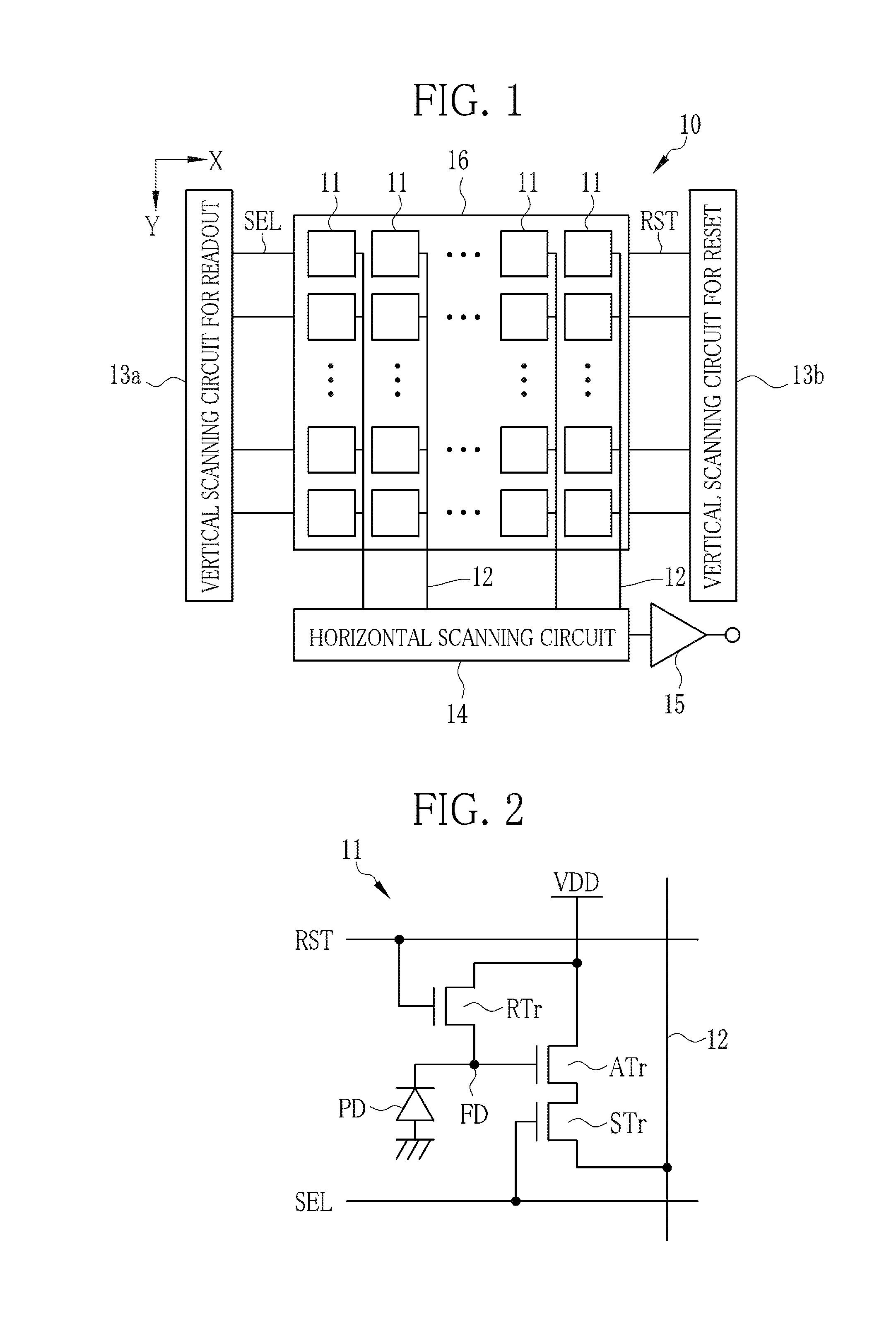
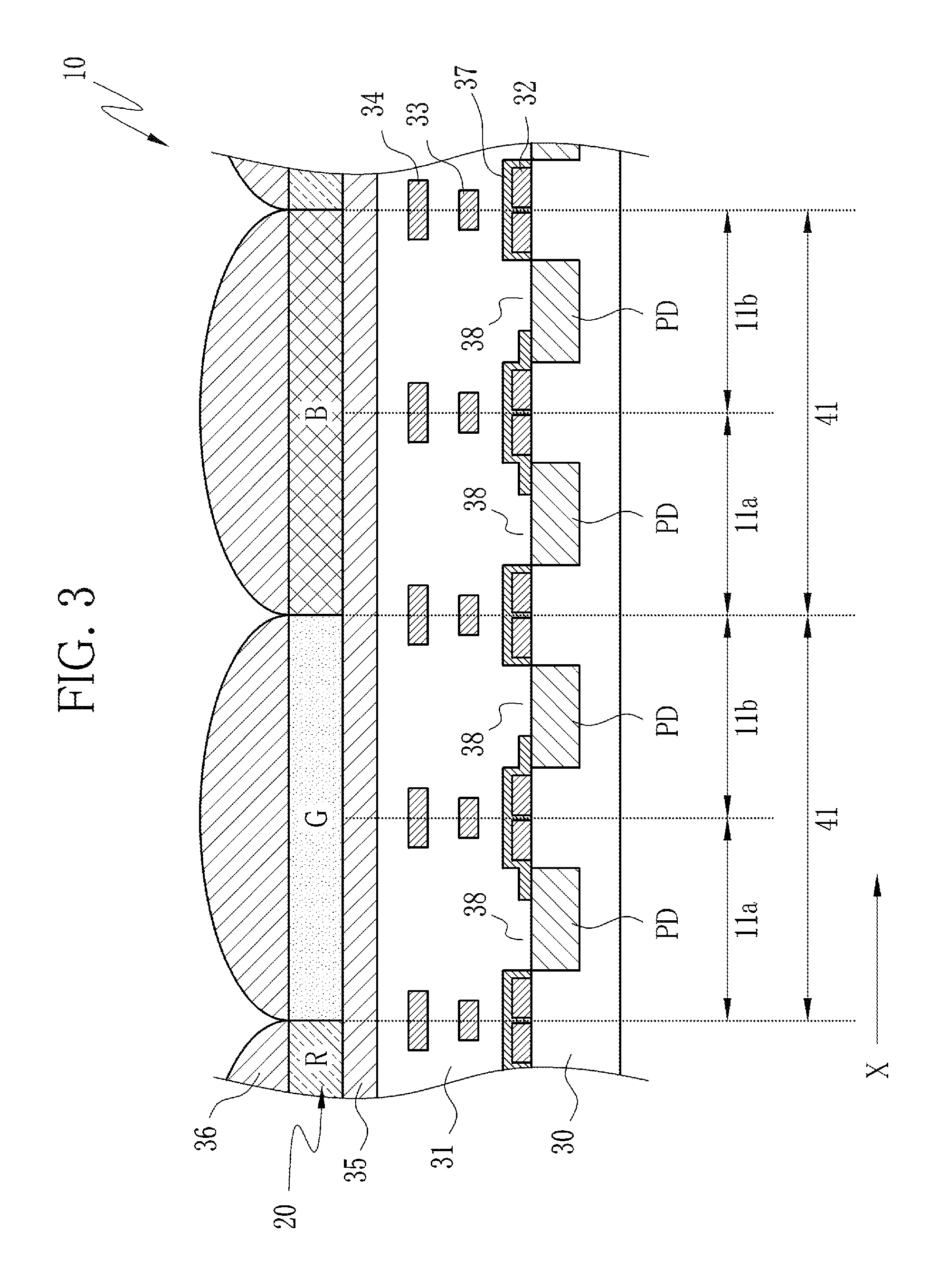
[0038]The pixels 11 are arranged in a semiconductor substrate in two dimensions along a horizontal direction (X direction) and a vertical direction (Y direction). The pixel 11 has a photodiode (photoelectric conversion element) for producing electric charge in accordance with the amount of light received thereby and a plurality of transistors (see FIG. 2). Every pixel 11 is a phase difference pixel that has selectivity in an incident angle in the horizontal direction, depending on the position of an opening formed in a light shielding film contai...


PUM


Abstract

A color filter array has G filters, R filters, and B filters. A pair of phase difference pixels adjoining in a horizontal direction is provided with one of the G, R, and B filters. In the color filter array, a fundamental array pattern, including the G, R, and B filters, is repeatedly disposed in horizontal and vertical directions. The G filters, which most greatly contributes to obtainment of luminance information, are disposed in every line extending in the horizontal direction, the vertical direction, and slanting directions. Both of the R filters and the B filters are disposed in every line extending in the slanting directions. The number of the G filters is larger than that of the R filters or the B filters.

Description

CROSS-REFERENCE TO RELATED APPLICATIONS[0001]This application is a continuation of PCT International Application No. PCT / JP2012 / 083582 filed on Dec. 26, 2012, which claims priority under 35 U.S.C §119(a) to Japanese Patent Application No. 2011-285902 filed on Dec. 27, 2011. Each of the above applications is hereby expressly incorporated by reference, in its entirety, into the present application.BACKGROUND OF THE INVENTION[0002]1. Field of the Invention[0003]The present invention relates to a single-panel type solid-state imaging device for taking a stereoscopic image.[0004]2. Description Related to the Prior Art[0005]In a single-panel type solid-state imaging device, a color filter array is disposed on a substrate that is formed with a two-dimensional array of photoelectric conversion elements (photodiodes). The color filter array has a plurality of color filters patterned in a mosaic, and each photoelectric conversion element is opposed to the color filter of a specific color. Eac...

Claims


Application Information

Patent Timeline
IPC IPC(8): H04N13/02H01L27/146
CPCH04N13/0217H04N13/0207H01L27/14621H04N13/0257H04N2209/045H04N13/207H04N13/218H04N13/257H04N23/843H04N25/134
Inventor OKIGAWA, MITSURUHAYASHI, KENKICHITANAKA, SEIJI
Owner FUJIFILM CORP
Why Eureka
Try Eureka