High-speed, High-density, and Low-power consumption Phase-change Memory Unit, and Preparation Method Thereof

US20140291597A1Inactive Publication Date: 2014-10-02SHANGHAI INST OF MICROSYSTEM & INFORMATION TECH CHINESE ACAD OF SCI
18 Cites 4 Cited by

Patent Information

Authority / Receiving Office
US · United States
Current Assignee / Owner
Publication Date
2014-10-02
Estimated Expiration
Not applicable · inactive patent

Smart Images

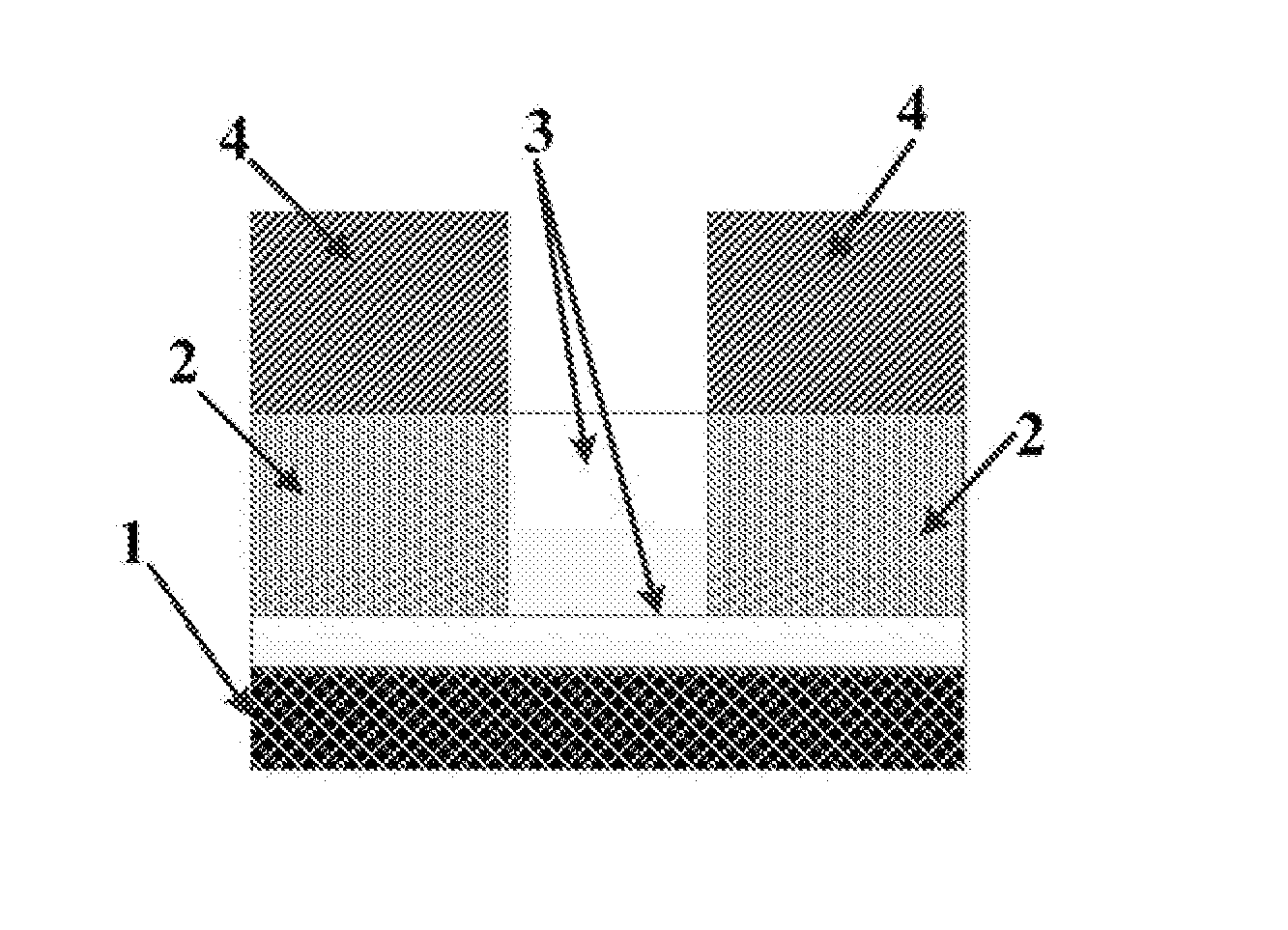
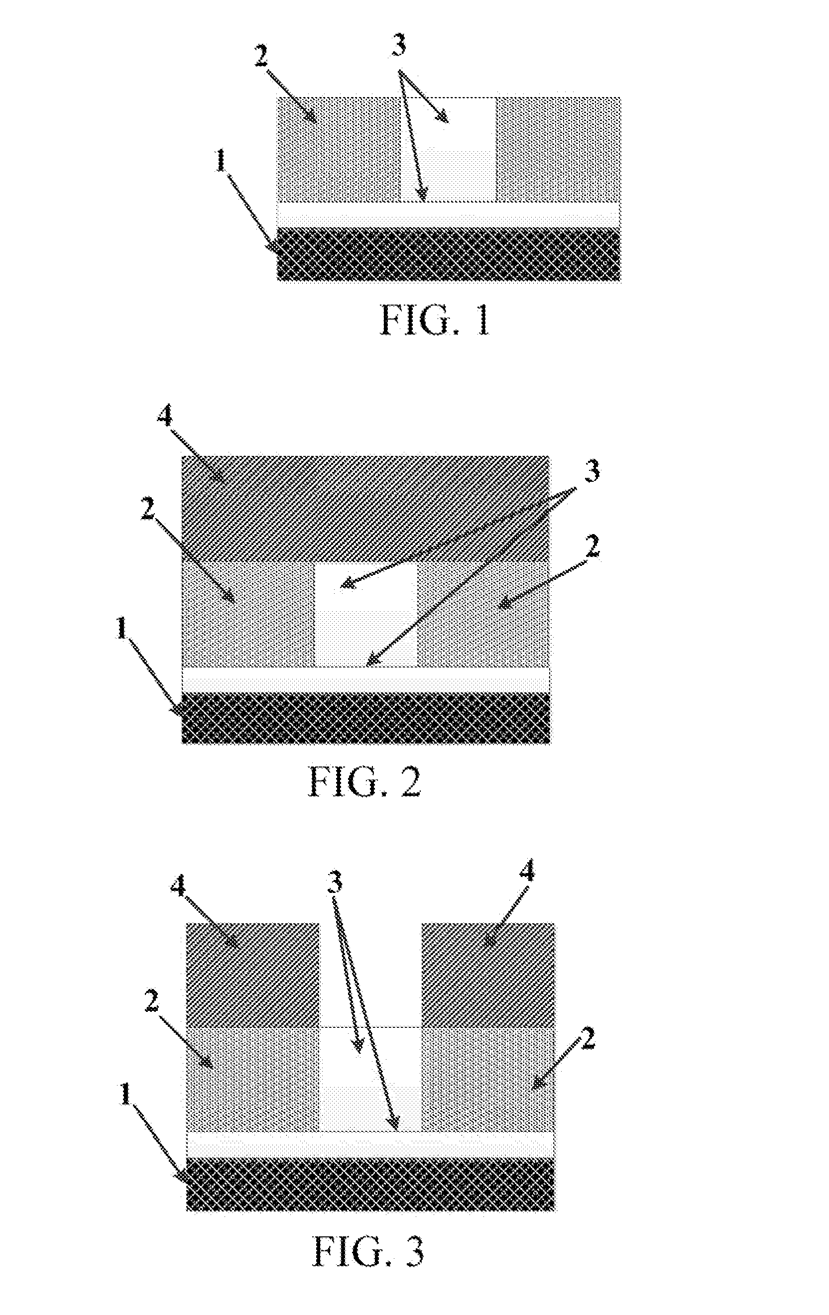
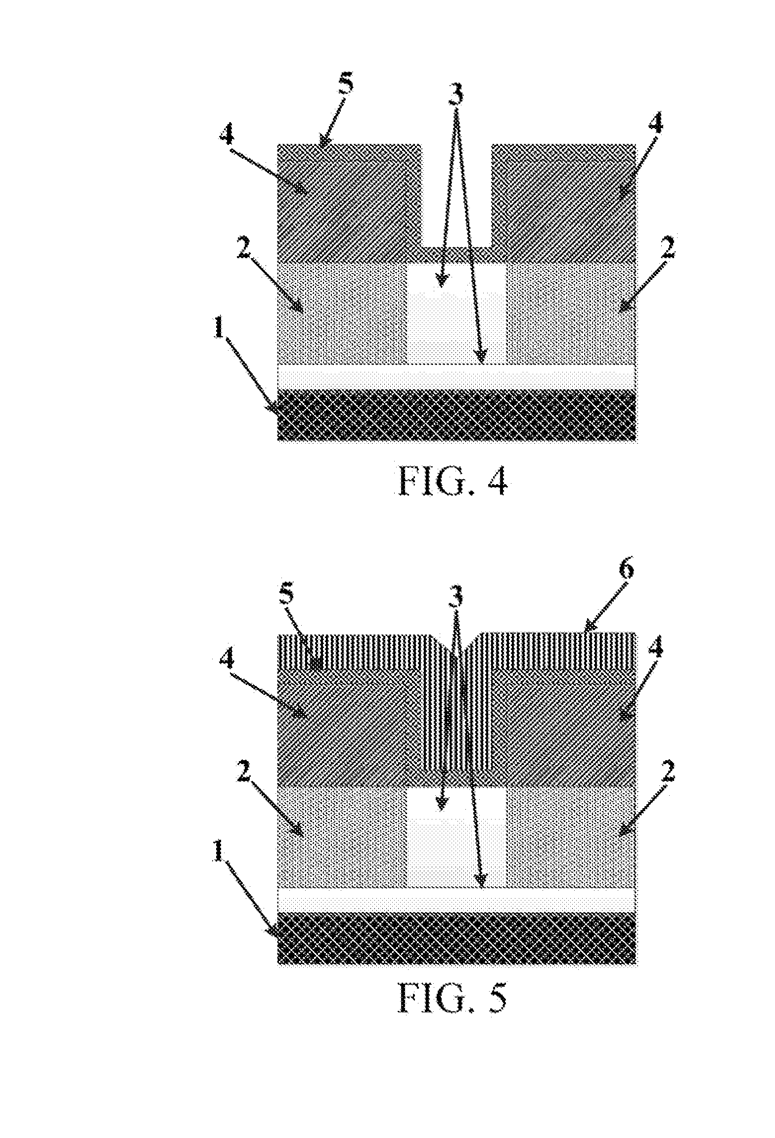
  • Figure 1
    Figure 1
  • Figure 2
    Figure 2
  • Figure 3
    Figure 3
Patent Text Reader

Abstract

The present invention provides a high-speed, high-density, and low-power consumption phase-change memory unit, and a preparation method thereof In the preparation method of the present invention, a transition material layer with an accommodation space is first prepared on a surface of a structure of a formed first electrode, where the accommodation space corresponds to the first electrode; a phase-change material layer is then prepared on a structure of the formed transition material layer, and the phase-change material layer is enabled to be in the accommodation space; and afterwards, a second electrode material layer is prepared on a surface of a structure of the prepared phase-change material layer, so as to prepare a phase-change memory unit; where phase-change material layer and the first electrode are isolated from each other by the transition material layer, and the second electrode material layer is in electrical communication with the phase-change material layer.
Need to check novelty before this filing date? Find Prior Art

Description

BACKGROUND OF THE PRESENT INVENTION

[0001] 1. Field of Invention

[0002] The present invention relates to the field of phase-change memories, and more specifically to a high-speed, high-density, and low-power consumption phase-change memory unit, and a preparation method thereof.

[0003] 2. Description of Related Arts

[0004] In the semi-conductor market, memories are of great importance. At present, the memories are mainly classified: static random access memories (SRAMs), dynamic random access memories (DRAMs), magnetic disks, flash memories (Flashes), and ferroelectric memories. Other memories such as phase change random access memories (PCRAMs) and resistive random access memories (RRAMs), as candidates of the next-generation memory, also receive much attention. In the industry, it is considered that FLASH will encounter restrictions in size. Among various memory technologies that probably replace the current memory technologies and become novel commercial memory technologies, the PCRAM is...

Examples

Embodiment Construction

[0029]The implementation of the present invention is described in the following through specific examples, and persons skilled in the art can easily understand other advantages and effects of the present invention through the content disclosed in the specification. The present invention may also be executed or applied through other different examples, modifications and variations may be made to the details in the specification on the basis of different opinions and applications without departing from the principle of the present invention.

[0030]Referring to FIG. 1 to FIG. 10, it should be noted that, the drawings provided in the embodiment merely exemplarily describes a basic concept of the present invention, so components related to the present invention are merely shown in the drawings, but are not drawn according to the number, shapes and size of the components in actual implementation. The shape, the number and the size of the components can be changed at will in the actual impl...