Power supply circuit

a power supply circuit and power supply technology, applied in the field of power supply circuits, can solve the problems of large current requirements of the signal processor, especially in reading and writing data, and achieve the effect of improving output voltage accuracy and stable operation of load

Active Publication Date: 2014-10-23
ROHM CO LTD
View PDF0 Cites 10 Cited by
  • Summary
  • Abstract
  • Description
  • Claims
  • Application Information

AI Technical Summary

Benefits of technology

[0010]Therefore, it is an object of the present invention to provide a power supply circuit contributing to stable operation of a load (for example, by suppressing a transient decrease of an output voltage or by improving an output voltage accuracy).

Problems solved by technology

For instance, when a signal processor configured to perform signal processing on data of a magnetic disk is a load of the power supply circuit, the signal processor requires large current particularly in reading and writing data.

Method used


Image

  • Power supply circuit
  • Power supply circuit
  • Power supply circuit

Examples


first embodiment

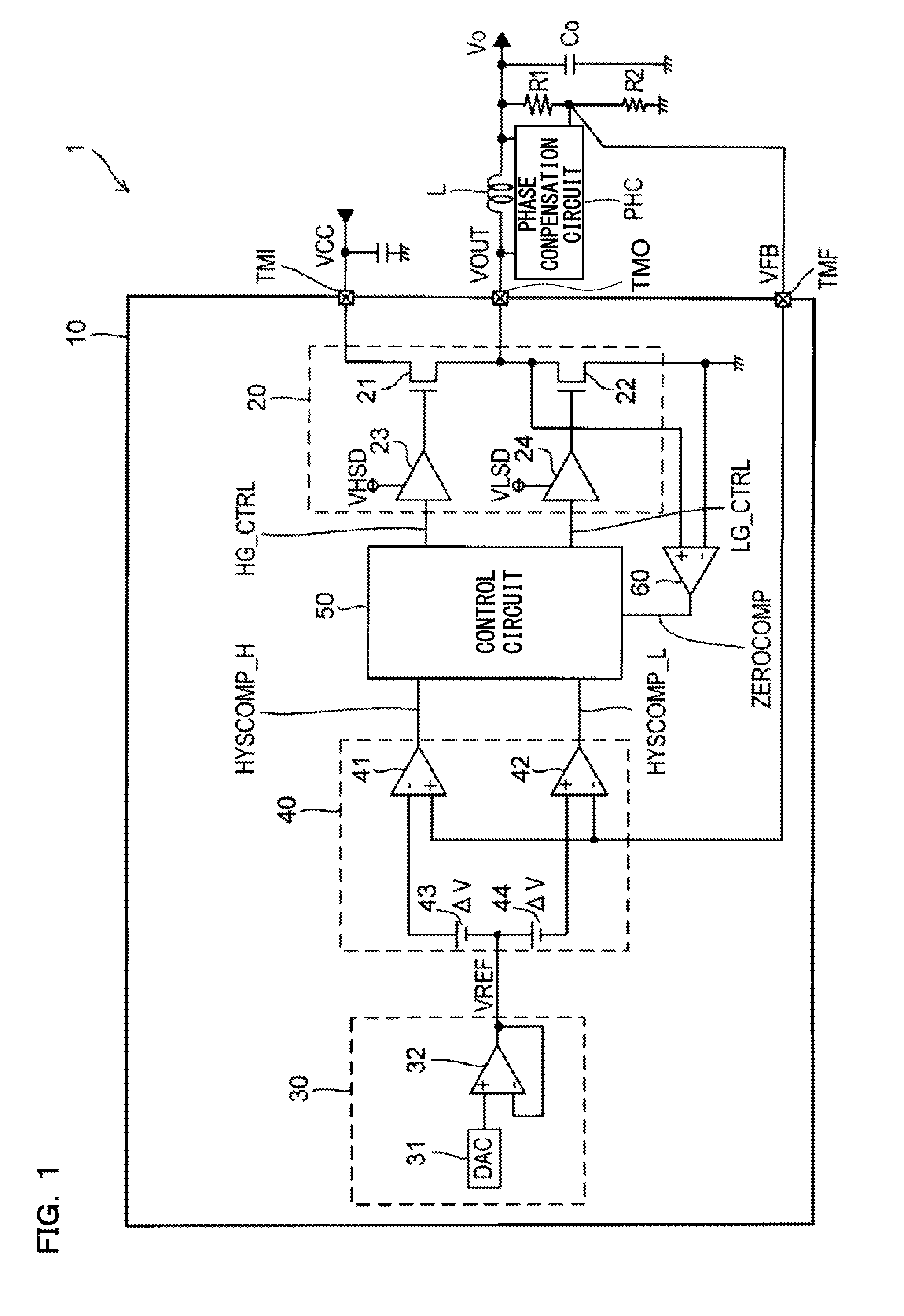
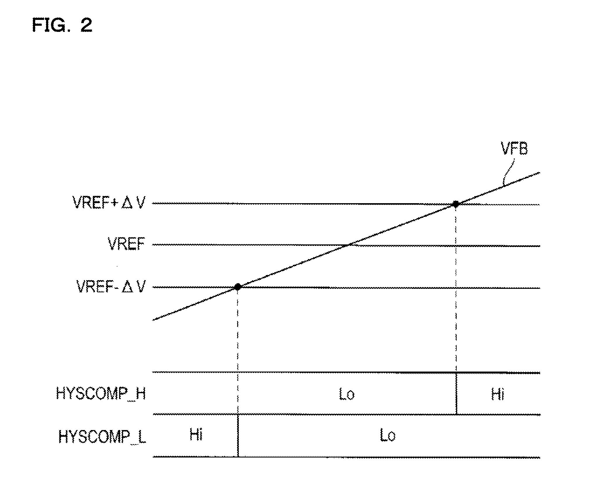
[0035]A first embodiment of the present invention is described. FIG. 1 is a schematic diagram of a power supply circuit 1 corresponding to the first embodiment of the present invention. The power supply circuit 1 generates from a DC input voltage a DC output voltage having a voltage value different from that of the input voltage. It is possible to consider that VOUT described later is the output voltage, but it is considered here that Vo described later is the output voltage. The input voltage is denoted by VCC. The input voltage VCC and the output voltage Vo are positive voltages. However, it is possible to modify the structure of the power supply circuit 1 so that the input voltage VCC and the output voltage Vo are negative voltages (the same is true in other power supply circuits described later). In addition, a potential to be a reference of individual voltages such as the input voltage VCC and the output voltage Vo is referred to as a reference potential, and a wiring, a metal ...

second embodiment

[0051]A second embodiment of the present invention is described. When i is an arbitrary natural number, the (i+1)th embodiment is an embodiment based on the first to the i-th embodiments. Concerning a matter that is not described in the (i+1)th embodiment, the descriptions in the first to the i-th embodiments are also applied to the (i+1) embodiment unless otherwise noted and as long as no contradiction arises.

[0052]It is possible to dispose in the IC 10 a plurality of unit blocks, each of which includes the output circuit 20, the reference voltage generation circuit 30, the comparing circuit 40, the control circuit 50, and the comparator 60 (see FIG. 1). In this case, for each unit block, the terminals TMI, TMO, and TMF are disposed in the IC 10, and each unit block is equipped with an analog block including the inductor L, the voltage dividing resistors R1 and R2, the output capacitor Co, and the phase compensation circuit PHC. Thus, the output voltages Vo for the number of the un...

third embodiment

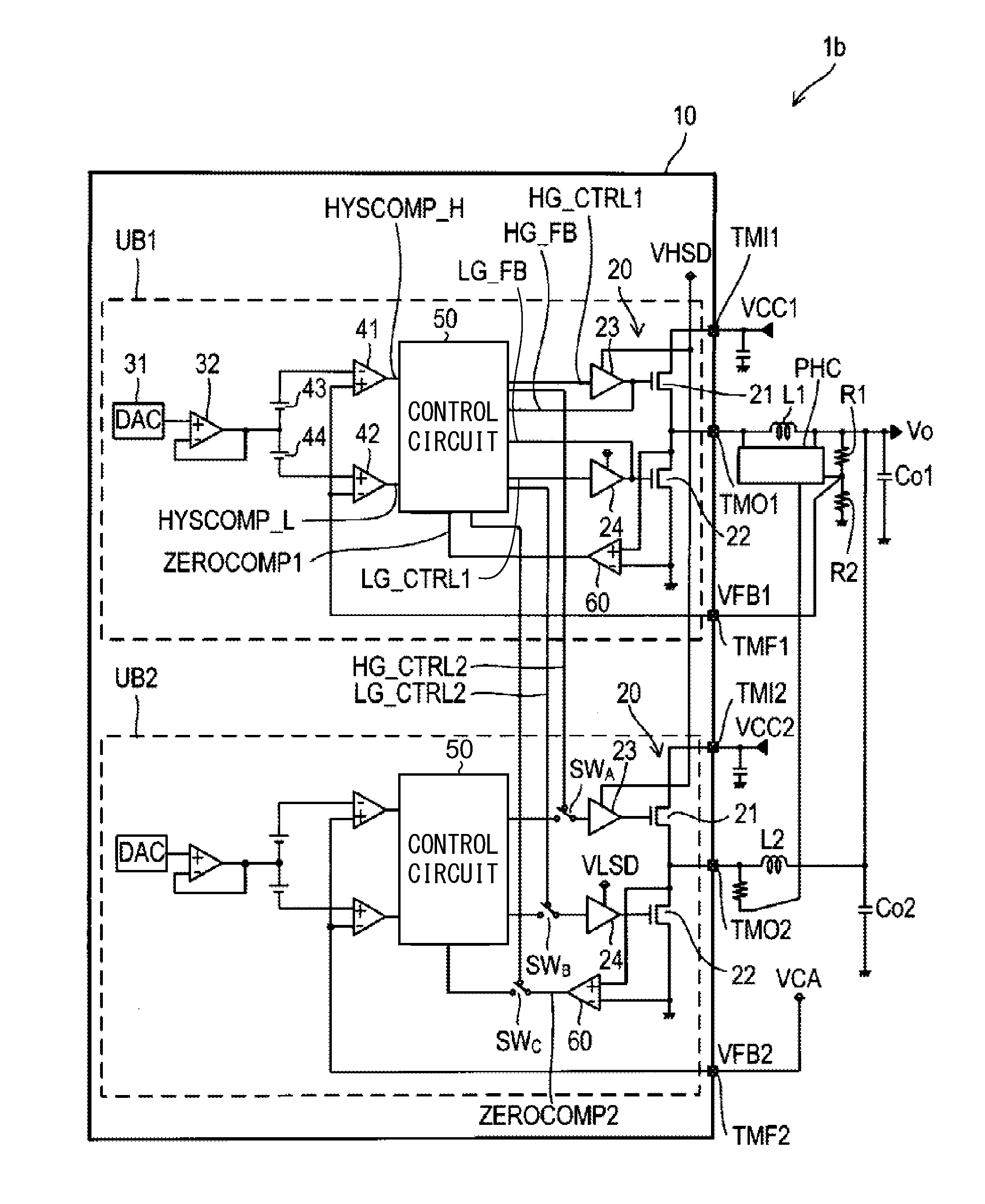
[0057]A third embodiment of the present invention is described. FIG. 5 illustrates a schematic diagram of a power supply circuit 1b according to the third embodiment. The power supply circuit 1b also uses the IC 10 described above in the second embodiment. However, the power supply circuit 1b can realize parallel driving in which a plurality of the output circuits 20 are used in parallel so as to obtain one output voltage Vo.

[0058]In the power supply circuit 1b, the inductor L and the output capacitor Co (see also FIG. 1) disposed for the unit block UB1 are denoted by L1 and Co1, respectively, while the inductor L and the output capacitor Co disposed for the unit block UB2 are denoted by L2 and Co2, respectively. In the unit block UB1, the terminal TMO1 connected commonly to the source of the FET 21 and the drain of the FET 22 is connected to the positive electrode of the capacitor Co1 via the inductor L1. In the unit block UB2, the terminal TMO2 connected commonly to the source of ...


PUM


Abstract

Each of unit blocks (UB1, UB2) is provided with an output circuit (20) including a serial circuit of FETs (21) and (22). A power supply circuit (1b) can operate in a first mode for generating an output voltage (Vo) using only one of the output circuits (20) or in a second mode for generating the output voltage (Vo) using two output circuits (20) by synchronous / parallel driving. When switching from the first mode to the second mode, start of the synchronous / parallel driving from a state where the FET (22) on the low voltage side is turned on is inhibited (start of the synchronous / parallel driving is waited until the FET (21) on the high voltage side is turned on).

Description

CROSS-REFERENCE TO RELATED APPLICATIONS[0001]This application is based on Japanese Patent Application No. 2013-090442 filed on Apr. 23, 2013, the contents of which are hereby incorporated by reference.BACKGROUND OF THE INVENTION[0002]1. Field of the Invention[0003]The present invention relates to a power supply circuit.[0004]2. Description of Related Art[0005]A power supply circuit illustrated in FIG. 19 uses an output circuit 910 including a serial circuit of a high side FET disposed on a high voltage side and a low side FET disposed on a low voltage side, so as to generate an output voltage Vo′ from an input voltage. In the power supply circuit illustrated in FIG. 19, each FET is controlled to turn on and off based on a feedback voltage VFB′ corresponding to the output voltage Vo′.[0006]In this case, as illustrated in FIG. 20, the feedback voltage VFB′ is compared with each of voltages (VREF′+ΔV) and (VREF′−ΔV), and the FETs are controlled to turn on and off based on the compariso...

Claims


Application Information

Patent Timeline
Patent Type & Authority Applications(United States)
IPC IPC(8): H02M5/293
CPCH02M2005/2932H02M5/293H02M3/1584H02M3/1566
Inventor NAKABAYASHI, HIROTAKA
Owner ROHM CO LTD
Why Eureka
Try Eureka