Power conversion device

a power conversion device and power technology, applied in the direction of dc-dc conversion, dc-dc conversion, efficient power electronics conversion, etc., can solve the problems of high noise, element destruction, and voltage surge occurring at either end of the element when switching is a considerable problem,

Active Publication Date: 2014-10-30
FUJI ELECTRIC FA COMPONENTS & SYST CO LTD
View PDF25 Cites 50 Cited by
  • Summary
  • Abstract
  • Description
  • Claims
  • Application Information

AI Technical Summary

Benefits of technology

[0016]Embodiments of the invention provide a power conversion device such that it is possible to realize both a suppression of switching surge and a countermeasure to noise in a power conversion device having a semiconductor switching element.
[0018]In the heretofore described power conversion device, an IGBT is used as the semiconductor switching element in the power conversion portion. Further, a noise suppression capacitor whose capacitance is smaller than that of the snubber capacitor, and which has a capacitance larger than the output capacitance between main electrodes (between the collector and emitter) of the IGBT, being included as the interline capacitor, there is a reduction in conduction noise and radiation noise components accompanying series resonance occurring in the direct current power supply line portion and power conversion portion.
[0021]The heretofore described power conversion device is such that, as a resistor is connected in series with the interline capacitor (noise suppression capacitor), it is possible to effectively attenuate noise accompanying series resonance with the resistor.
[0023]The heretofore described power conversion device is such that a noise suppression capacitor and a resistor connected in series with the capacitor can be configured in a semiconductor module, and a compact and effective suppression of noise is thus possible, without the noise suppression capacitor and resistor being connected to a wiring pattern or bus bar.
[0025]The power conversion device of the invention is such that conduction noise and radiation noise components accompanying series resonance occurring in the direct current power supply line portion and power conversion portion are reduced by parallel resonance occurring because of the capacitance components of the interline capacitor, the parasitic inductance components of the snubber capacitor, and the inductance components of the peripheral direct current power supply lines. Also, the power conversion device of the invention is such that, by the snubber capacitor and interline capacitor being added, the impedance of the direct current power supply lines is smaller than that in a heretofore known power conversion device, and the switching surge does not worsen.
[0026]Because of this, the power conversion device of the invention is such that it is possible to simultaneously realize a suppression of switching surge and a suppression of radiation noise and conduction noise, which has considerable advantages from a practical perspective.

Problems solved by technology

A power conversion device configured to use a semiconductor switching element is such that a voltage surge occurring at either end of the element when switching is a considerable problem.
Further, when the switching surge exceeds the breakdown voltage of the semiconductor switching element, it may lead to element destruction, which has a considerable effect on the reliability of the power conversion device.
Also, the sharp changes in voltage and current caused when switching, and a resonance phenomenon occurring in accompaniment to the sharp changes, cause a high level of noise, resulting in conduction noise conducted to the power supply system, and radiation noise propagated to a space on the periphery of the power conversion device and a cable connected to the device.
Herein, Lp1, Lp2, Lp3, Ldcp, Ldcn, Ln1, Ln2, and Ln3 in FIG. 19 are line inductors that exist in printed patterns or bus bars configuring the direct current power supply lines of the converter and inverter, and are a main cause of switching surge occurring.
Further, the larger the values of the line inductors, the larger the switching surge becomes.
However, even when adding this kind of snubber circuit, it is often the case that it is difficult to sufficiently reduce conduction noise and radiation noise.
Meanwhile, it may happen that the switching surge, not converging immediately after the peak value, resonates and oscillates.
Although this kind of resonance phenomenon is not a cause of element destruction, it is a cause of the occurrence of noise that causes an extremely high value in a frequency spectrum, as shown in FIG. 21, and results in the occurrence of large radiation noise or conduction noise.
However, a power conversion device described in JP-A-2010-41790 is such that there is also parasitic inductance in the capacitor connected in parallel to the direct current power supply line, and there is concern that the value of that inductance is generally greater than the inductance value of the direct current power supply line with which the capacitor is connected in parallel.
Because of this, it is difficult to reduce the high level conduction noise and radiation noise.

Method used


Image

  • Power conversion device
  • Power conversion device
  • Power conversion device

Examples


example 1

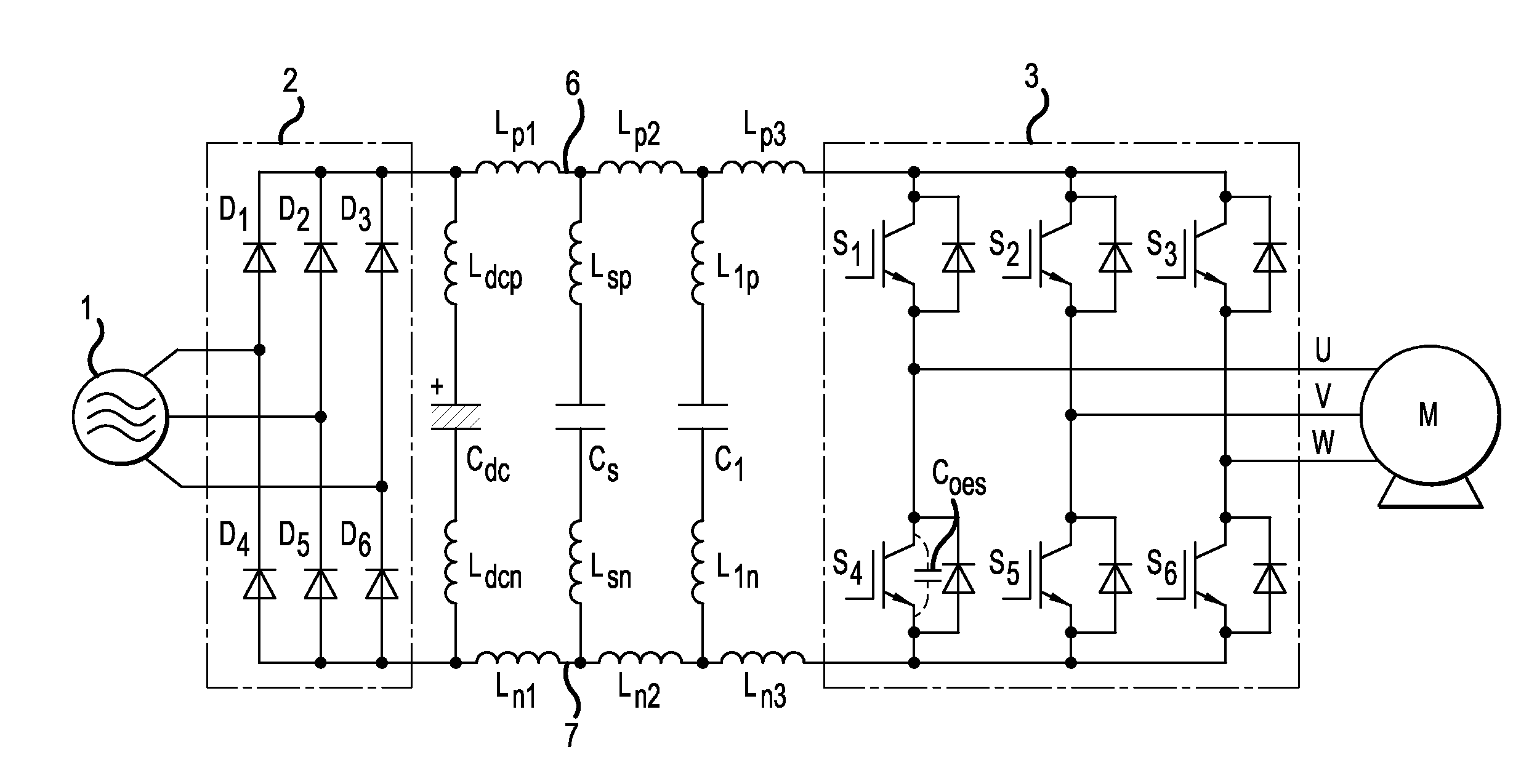
[0049]FIG. 1 is a circuit diagram showing a configuration of a power conversion device according to an Example 1 of the invention. Example 1 differs from the heretofore known power conversion device shown in FIG. 20 in that a noise suppression capacitor (interline capacitor) C1 that suppresses conduction noise and radiation noise is included between a snubber capacitor Cs between a positive line 6 and negative line 7, which are direct current power supply lines, and an inverter 3, and that the capacitance of the noise suppression capacitor C1 is of a value smaller than that of the capacitance of the snubber capacitor Cs, and of a value greater than that of a capacitance Coes (output capacitance) between main electrodes (between a collector and an emitter) of semiconductor switching elements (IGBTs; S1 to S6) used in the inverter 3.

[0050]A film capacitor may be used as the snubber capacitor Cs, and a ceramic capacitor may be used as the noise suppression capacitor C1.

[0051]Herein, as...

example 2

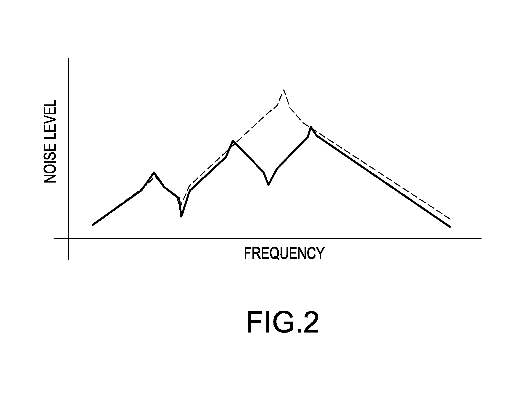
[0066]In the circuit configuration of Example 1 of the invention shown in FIG. 1, series resonance is generated in a series circuit formed of inductance components, being parasitic inductance components (L1p and L1n) included in the noise suppression capacitor C1, the inductance components (not shown) in the power module, and the inductance components (Lp3 and Ln3) of the direct current power supply lines 6 and 7, and of the capacitance components, being the output capacitance Coes of the IGBTs (S1 to S6) and the noise suppression capacitor C1. Noise exceeding a desired noise level may occur in accompaniment to the series resonance.

[0067]In this case, it is good when a resistor R1 is connected in series with the noise suppression capacitor C1, and the series circuit is connected between the power supply lines 6 and 7 nearest to the inverter 3, as depicted in a circuit diagram showing an Example 2 of the invention in FIG. 8. By adopting this kind of circuit configuration, it is possi...

example 3

[0068]Example 3 differs from Examples 1 and 2 in that, as shown in FIG. 9, the noise suppression capacitor C1, which has capacitance of a value smaller than that of the capacitance of the snubber capacitor Cs and greater than the output capacitance Coes of the IGBTs (S1 to S6) configuring the power conversion portion, and another noise suppression capacitor C2, which has capacitance of a value smaller than that of the noise suppression capacitor C1 and capacitance greater than the output capacitance Coes of the IGBTs (S1 to S6), are connected between the direct current power supply lines 6 and 7. That is, the circuit configuration is such that the plurality of noise suppression capacitors C1 and C2, whose capacitance becomes smaller the nearer they are to the switching elements configuring the power conversion portion and whose capacitance becomes larger the nearer they are to the snubber capacitor Cs, are connected between the direct current power supply lines 6 and 7.

[0069]By so d...


PUM


Abstract

A power conversion device including a power conversion portion that switches direct current voltage supplied by a positive line and negative line of a direct current power supply with a semiconductor switching element, and outputs converted voltage, is such that a plurality of interline capacitors are connected in parallel between the positive line and negative line, the capacitance of the plurality of interline capacitors is of a value that becomes smaller the nearer to the power conversion portion the position in which the interline capacitor is connected, and the capacitance of the interline capacitor with the smallest value of capacitance is set to a value greater than that of the capacitance between main electrodes when a direct current voltage is applied to the switching element used in the power conversion portion.

Description

CROSS-REFERENCE TO RELATED APPLICATIONS[0001]This application is a continuation of International Application No. PCT / JP2012 / 001487, filed on Mar. 5, 2012, the disclosure of which, in its entirety, including the drawings, claims, and the specification thereof, is incorporated herein by reference.FIELD OF THE INVENTION[0002]The present invention relates to a power conversion device, and in particular, relates to technology of suppressing surge voltage and electromagnetic noise generated by the power conversion device.BACKGROUND ART[0003]A power conversion device configured to use a semiconductor switching element is such that a voltage surge occurring at either end of the element when switching is a considerable problem. When the semiconductor switching element is, for example, an IGBT, the voltage surge occurs between the collector and emitter (hereafter, this kind of voltage surge will be called a switching surge).[0004]The relationship between a collector-to-emitter voltage Vce occ...

Claims


Application Information

Patent Timeline
Patent Type & Authority Applications(United States)
IPC IPC(8): H02M5/458
CPCH02M5/458H02M1/14H02M7/5387H02M1/44H02M7/003Y02B70/10H02M1/348H02M1/346H02M3/01H02M3/33573
Inventor FUJITA, MIWAKOKAIMI, TAKASHI
Owner FUJI ELECTRIC FA COMPONENTS & SYST CO LTD
Why Eureka
Try Eureka