Dark Current Reduction for Back Side Illuminated Image Sensor

Active Publication Date: 2014-10-30
TAIWAN SEMICON MFG CO LTD
View PDF0 Cites 1 Cited by
  • Summary
  • Abstract
  • Description
  • Claims
  • Application Information

AI Technical Summary

Benefits of technology

The patent describes an apparatus that includes a semiconductor image sensor device. This device has two different regions: a non-scribe-line region and a scribe-line region. The non-scribe-line region has a first substrate portion that contains a doped region that can detect radiation. The second substrate portion, which is in the scribe-line region, has the same material composition as the first substrate portion. The technical effect of this design is the improved detection and processing of images captured using the semiconductor image sensor device.

Problems solved by technology

However, conventional methods of forming color filters for BSI image sensor devices have been prone to suffer from thermal expansion issues, particular in a scribe line region of the BSI image sensor device.
Such thermal expansion may cause lateral stress to a photo-sensitive region of the image sensor and degrade dark current performance of the image sensor.
Therefore, while existing semiconductor image sensors have been generally adequate for their intended purposes, they are not entirely satisfactory in every aspect.

Method used


Image

  • Dark Current Reduction for Back Side Illuminated Image Sensor
  • Dark Current Reduction for Back Side Illuminated Image Sensor
  • Dark Current Reduction for Back Side Illuminated Image Sensor

Examples


Embodiment Construction

[0008]It is to be understood that the following disclosure provides many different embodiments, or examples, for implementing different features of the invention. Specific examples of components and arrangements are described below to simplify the present disclosure. These are, of course, merely examples and are not intended to be limiting. Moreover, the formation of a first feature over or on a second feature in the description that follows may include embodiments in which the first and second features are formed in direct contact, and may also include embodiments in which additional features may be formed interposing the first and second features, such that the first and second features may not be in direct contact. Various features may be arbitrarily drawn in different scales for the sake of simplicity and clarity.

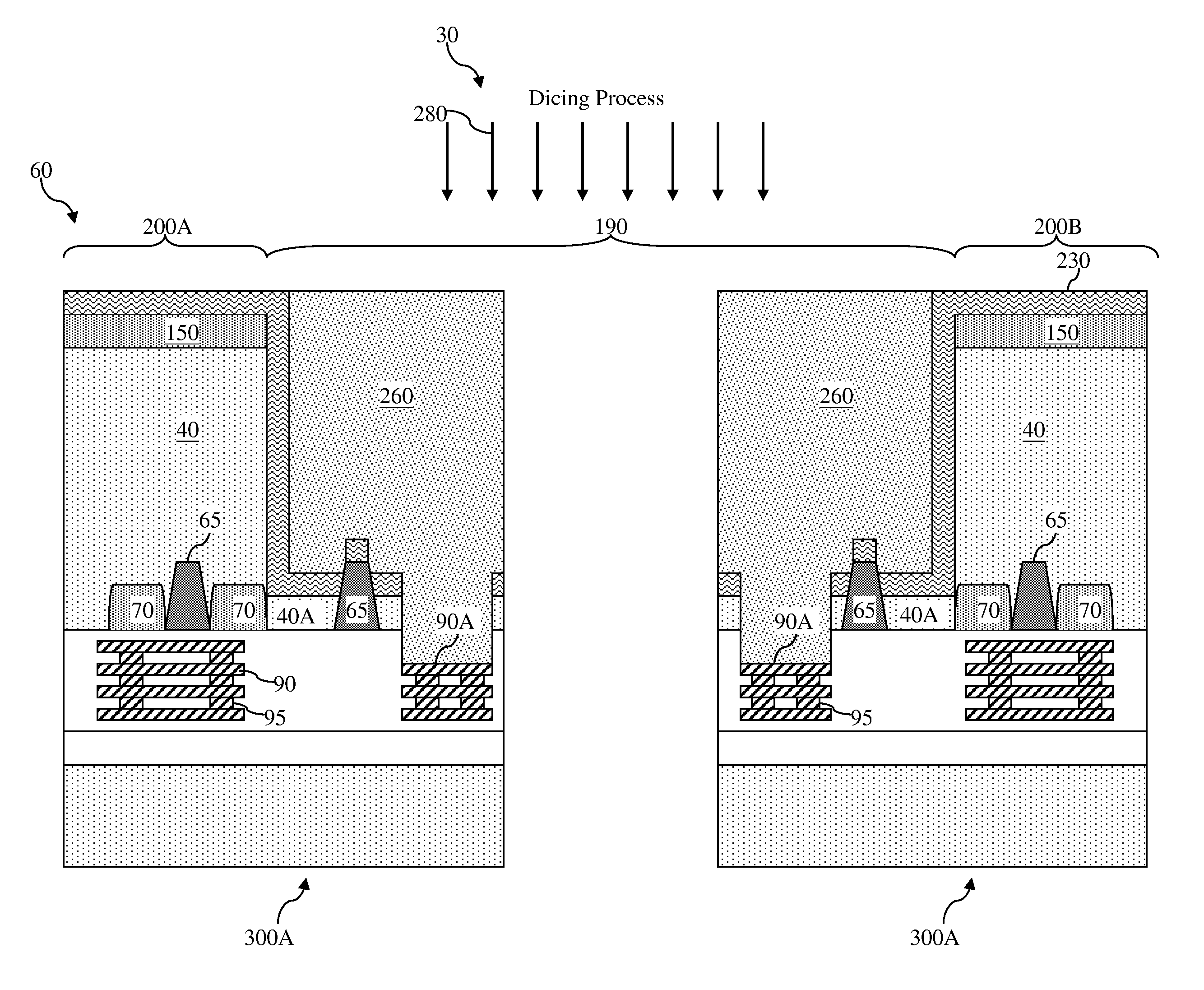
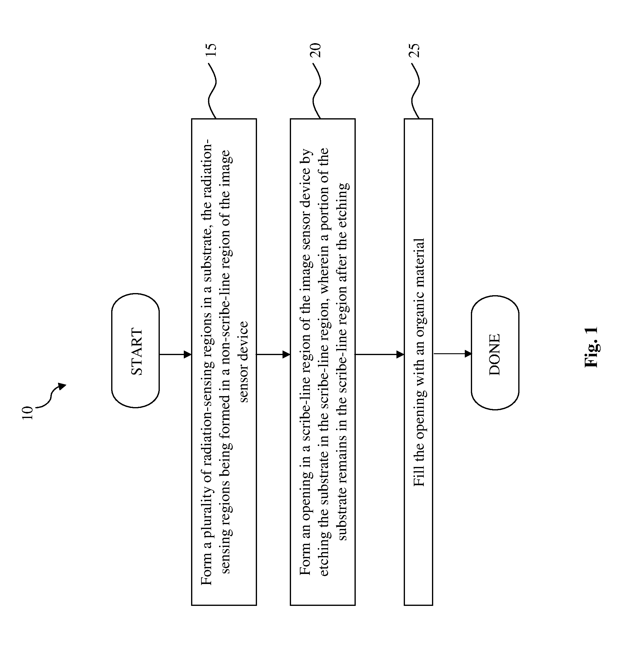
[0009]Illustrated in FIG. 1 is a flowchart of a method 10 for fabricating a semiconductor image sensor device according to various aspects of the present disclosure. Re...


PUM


Abstract

A method of fabricating a semiconductor image sensor device is disclosed. A plurality of radiation-sensing regions is formed in a substrate. The radiation-sensing regions are formed in a non-scribe-line region of the image sensor device. An opening is formed in a scribe-line region of the image sensor device by etching the substrate in the scribe-line region. A portion of the substrate remains in the scribe-line region after the etching. The opening is then filled with an organic material.

Description

PRIORITY DATA[0001]The present application is a divisional patent application of U.S. patent application Ser. No. 13 / 305,069, filed on Nov. 28, 2011, the disclosure of which is hereby incorporated by reference in its entirety.BACKGROUND[0002]Semiconductor image sensors are used to sense radiation such as light. Complementary metal-oxide-semiconductor (CMOS) image sensors (CIS) and charge-coupled device (CCD) sensors are widely used in various applications such as digital still camera or mobile phone camera applications. These devices utilize an array of pixels in a substrate, including photodiodes and transistors, that can absorb radiation projected toward the substrate and convert the sensed radiation into electrical signals.[0003]A back side illuminated (BSI) image sensor device is one type of image sensor device. These BSI image sensor devices are operable to detect light projected from the backside. The BSI image sensor devices include color filters for filtering a specific wave...

Claims


Application Information

Patent Timeline
IPC IPC(8): H01L27/146
CPCH01L27/14687H01L27/14632H01L27/1464H01L27/14685H01L27/14618H01L27/14621H01L27/14627H01L27/14636H01L27/14683H01L2924/0002H01L2924/00H01L27/14H04N25/63H01L27/1462H01L31/028
Inventor LU, SHOU-SHUHUANG, HSUN-YINGJUNG, HUANG-HSINCHIU, CHUN-MAOHSIAO, CHIA-CHICHANG, YUNG-CHENG
Owner TAIWAN SEMICON MFG CO LTD
Why Eureka
Try Eureka