Carrier substrate and manufacturing method thereof

a technology of carrier substrate and manufacturing method, which is applied in the manufacture of cable/conductor, printed circuit aspects, chemistry apparatus and processes, etc., can solve the problems of inability to accurately connect components with connection pads, and inability to easily distinguish connection pads from traces, etc., to achieve the effect of easy identification of connection pads for components

Active Publication Date: 2014-11-13
UNIMICRON TECH CORP
View PDF3 Cites 19 Cited by
  • Summary
  • Abstract
  • Description
  • Claims
  • Application Information

AI Technical Summary

Benefits of technology

[0007]The invention provides a carrier substrate and a manufacturing method thereof. The carrier substrate can allow the user to easily distinguish connection pads for components and can prevent the generation of oxidation phenomenon from exposed traces.

Problems solved by technology

Therefore, the arrangements not only affect electrical performance by readily generating oxidation phenomenon to the traces, the user also cannot easily distinguish the connection pads from the traces, and therefore the component cannot be directly connected with the connection pads accurately.

Method used


Image

  • Carrier substrate and manufacturing method thereof
  • Carrier substrate and manufacturing method thereof
  • Carrier substrate and manufacturing method thereof

Examples


Embodiment Construction

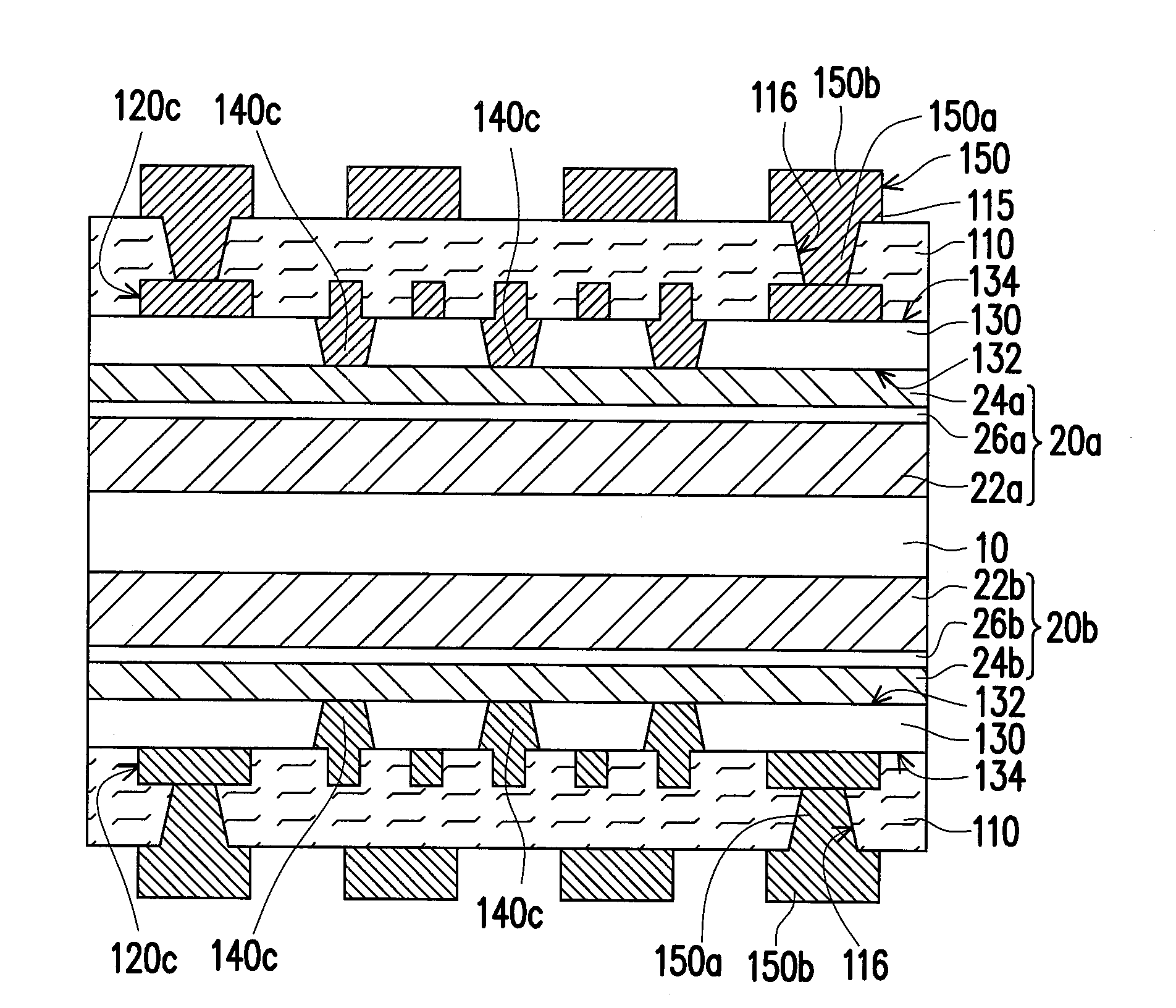
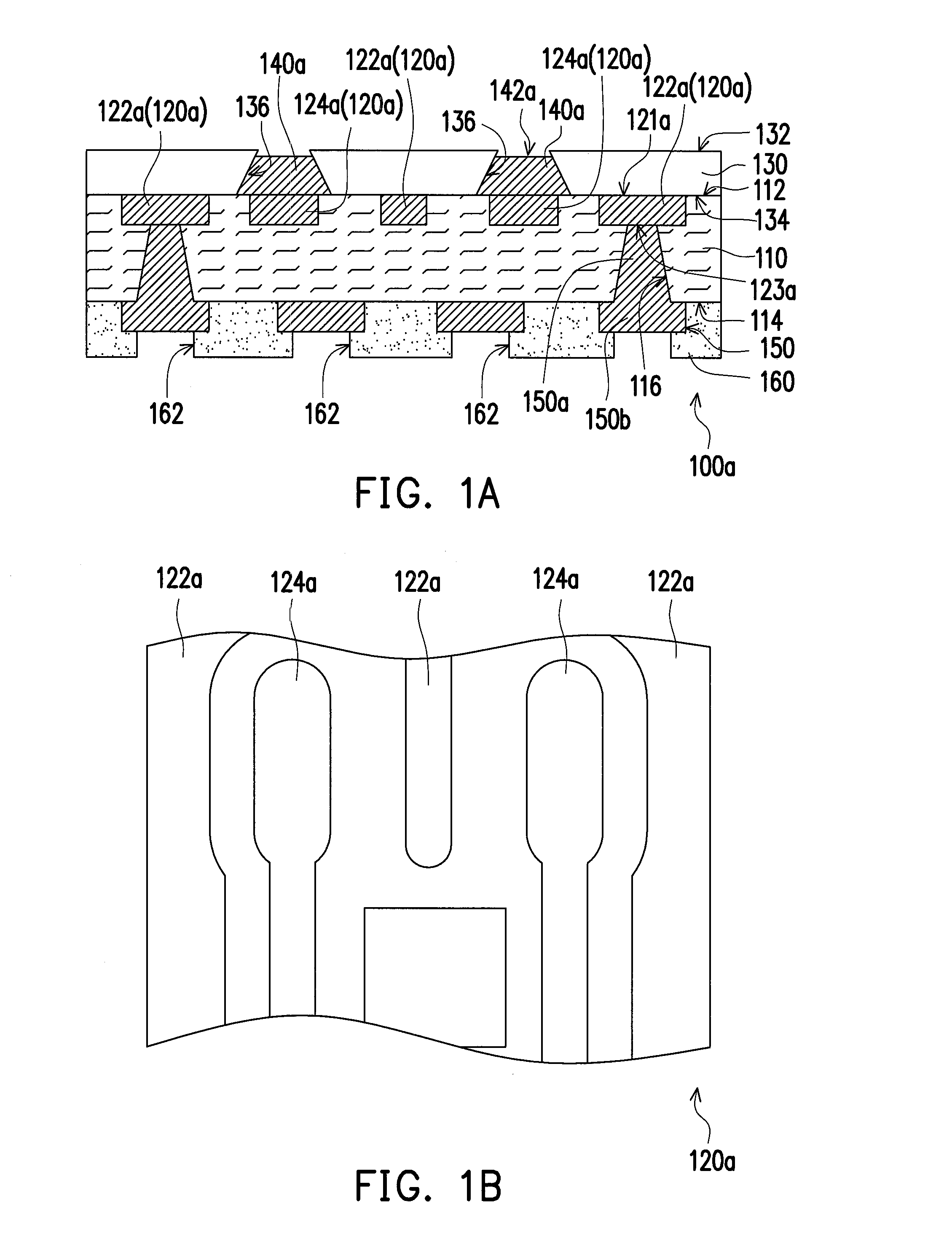
[0030]FIG. 1A illustrates a cross-sectional schematic diagram of a carrier substrate of an embodiment of the invention. FIG. 1B illustrates a schematic top view of the circuit layer of FIG. 1A. Referring first to FIG. 1A, in the present embodiment, a carrier substrate 100a includes a dielectric layer 110, a first circuit layer 120a, an insulation layer 130, a plurality of conductive blocks 140a, and a first conductive structure 150. Specifically, the dielectric layer 110 has two opposing surfaces 112 and 114 and a plurality of blind vias 116 (FIG. 1A schematically illustrates two). The first circuit layer 120a is embedded in the surface 112 of the dielectric layer 110 and has two opposing surfaces 121a and 123a, wherein the surface 121a is exposed from the surface 112 of the dielectric layer 110. The blind vias 116 extend from the surface 114 to the first circuit layer 120a and expose a portion of the surface 123a of the first circuit layer 120a. The insulation layer 130 has two opp...


PUM

PropertyMeasurementUnit
widthaaaaaaaaaa
conductiveaaaaaaaaaa
diameteraaaaaaaaaa

Abstract

A carrier substrate includes a dielectric layer, a first circuit layer, an insulation layer, conductive blocks, and a first conductive structure. The dielectric layer has a first surface, a second surface, and blind vias. The first circuit layer is embedded in the first surface and the blind vias extend from the second surface to the first circuit layer. The insulation layer is disposed on the first surface and has a third surface, a fourth surface, and first openings. The first openings expose the first circuit layer and an aperture of each first opening is increased gradually from the third surface to the fourth surface. The conductive blocks fill the first openings and connect with the first circuit layer. The first conductive structure includes conductive vias filling the blind vias and a second circuit layer disposed on a portion of the second surface.

Description

CROSS-REFERENCE TO RELATED APPLICATION[0001]This application claims the priority benefit of Taiwan application serial no. 102116226, filed on May 7, 2013. The entirety of the above-mentioned patent application is hereby incorporated by reference herein and made a part of this specification.BACKGROUND OF THE INVENTION[0002]1. Field of the Invention[0003]The invention relates to a substrate and a manufacturing method thereof, and more particularly, to a carrier substrate suitable for carrying components and a manufacturing method thereof[0004]2. Description of Related Art[0005]In recent years, with the rapid progress of the electronic technology, high-tech electronic industries have appeared one after another, thus more human-oriented, more performance-preferred electronic products are continuously evolving new things from the old, and have been designed to cater to the trend of being low-profiled and compact-sized. A carrier substrate is usually disposed in the electronic products. T...

Claims


Application Information

Patent Timeline
Patent Type & Authority Applications(United States)
IPC IPC(8): H05K1/11H05K3/46
CPCH05K1/112H05K3/4688H05K3/4015H05K3/0097H05K3/4644H05K2201/09827H05K2203/041H05K2203/1536
Inventor LIN, CHUN-TING
Owner UNIMICRON TECH CORP
Why Eureka
Try Eureka