Display device and manufacturing method thereof

a technology of a display device and a manufacturing method, applied in the field of display devices, can solve the problems of poor product quality of the display device, the inability to execute the process of the other display auxiliary members,

Active Publication Date: 2014-11-13
SHENZHEN CHINA STAR OPTOELECTRONICS TECH CO LTD
View PDF9 Cites 5 Cited by
  • Summary
  • Abstract
  • Description
  • Claims
  • Application Information

AI Technical Summary

Benefits of technology

[0008]One object of the present invention is to provide a manufacturing method for a display device such that the metho

Problems solved by technology

Due to the limitation imposed by the sintering process mentioned above (temperature greater than 500 degree Celsius on the cover of conventional OLED display devices), the processes of the other display auxiliary members

Method used


Image

  • Display device and manufacturing method thereof
  • Display device and manufacturing method thereof
  • Display device and manufacturing method thereof

Examples


Embodiment Construction

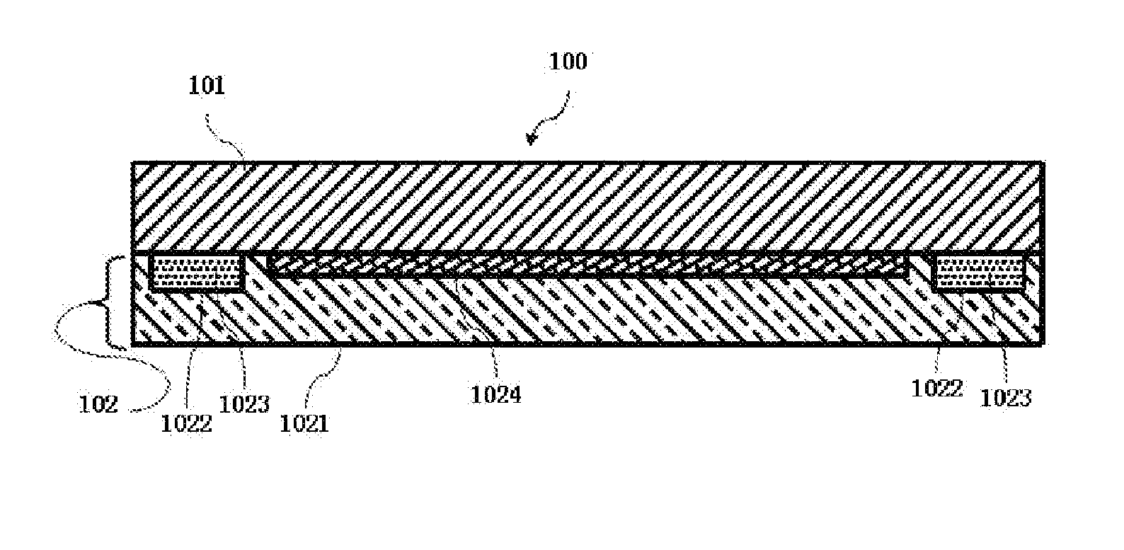
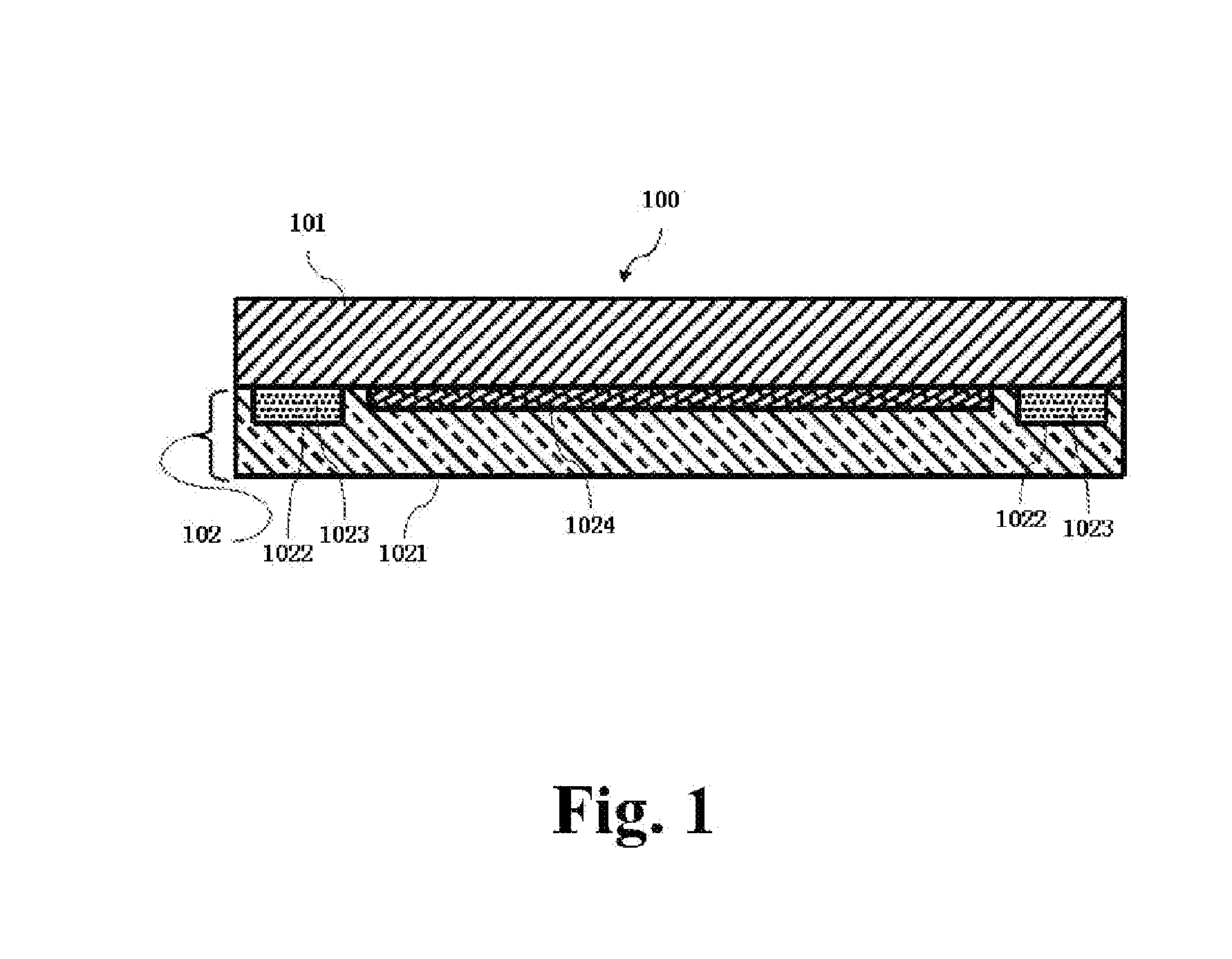
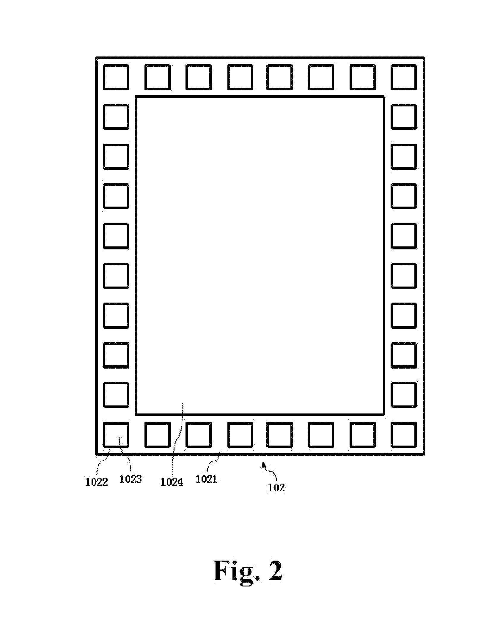
[0039]The following description of every embodiment, with reference to the accompanying drawings, is used to exemplify a specific embodiment which may be carried out in the present invention. Directional terms mentioned in the present invention, such as “top”, “bottom”, “front”, “back”, “left”, “right”, “inside”, “outside”, “side” etc., are only used with reference to the orientation of the accompanying drawings. Therefore, the used directional terms are intended to illustrate, but not to limit, the present invention. In the drawings, the components having similar structures are denoted by the same numerals.

[0040]A display device of the present invention compromises a display substrate and a cover, wherein the display substrate compromises: a substrate main body (not shown), a first electrode (not shown), an organic light emitting layer (not shown), and a second electrode (not shown). The first electrode, the organic light emitting layer and the second electrode are formed on the su...


PUM


Abstract

For a display device and manufacturing method for the display device, the method comprises steps of: disposing a plurality of recesses on the cover body; coating glass frit in the recesses; sintering the glass frit for forming sintered blocks; disposing display auxiliary members on the cover body having the sintered blocks formed thereon; and irradiating the sintered blocks by laser to combine the cover and the display substrate with the sintered blocks.
The present invention can prevent the display auxiliary members of the cover from being damaged in the packaging process of the display device.

Description

BACKGROUND OF THE INVENTION[0001]1. Field of Invention[0002]The present invention relates to a field of display technology. In particular, it pertains to a display device and a manufacturing method thereof.[0003]2. Description of Prior Art[0004]In conventional packaging process of an Organic Light Emitting Diode (OLED) display device, the glass frit applied on a cover is required to be sintered at a temperature greater than 500 degree Celsius for the packaging the cover and the display substrate.[0005]The Inventor finds that in practice the prior art exists at least the following problem:[0006]Due to the limitation imposed by the sintering process mentioned above (temperature greater than 500 degree Celsius on the cover of conventional OLED display devices), the processes of the other display auxiliary members cannot be executed, such as a color filter member process or a touch-sensitive member process). This is because the heat can damage the display auxiliary members, resulting in...

Claims


Application Information

Patent Timeline
IPC IPC(8): H01L51/56
CPCH01L51/56H10K50/8426H10K50/841H10K71/00
Inventor WU, TAI-PI
Owner SHENZHEN CHINA STAR OPTOELECTRONICS TECH CO LTD
Why Eureka
Try Eureka