Integrated circuit package with an interposer formed from a reusable carrier substrate

a technology of integrated circuits and carrier substrates, which is applied in the direction of electrical equipment, semiconductor devices, semiconductor/solid-state device details, etc., can solve the problems of difficult control of the thinning process, large stress on the 3d chip at operational temperatures, and high cost and time-consuming processes of thinning silicon interposer substrates, etc., to achieve greatly reduced parasitic capacitance in the integrated circuit package, and the effect of significantly reducing the siz

Inactive Publication Date: 2014-11-20
NVIDIA CORP
View PDF8 Cites 11 Cited by
  • Summary
  • Abstract
  • Description
  • Claims
  • Application Information

AI Technical Summary

Benefits of technology

[0010]One advantage of the above-described embodiment is that through-interposer vias in an integrated circuit package can be formed from a thin layer of semiconductor material removed from a reusable carrier substrate, and therefore can be scaled down significantly in size. Such reduced-size, through-interposer vias can be etched and filled much more cost-effectively and result in greatly reduced parasitic capacitance in the integrated circuit package. Moreover, because the interposer of the integrated circuit package can be formed from a layer of semiconductor material separated from a substrate rather than via a thinning process, the interposer can be advantageously fabricated without imprecise and difficult-to-control thinning operations.

Problems solved by technology

Etching openings in the silicon interposer substrate, depositing insulating dielectric and the conductive material in the openings, and thinning the silicon interposer substrate are all costly and time-consuming processes.
In addition, the thinning process is difficult-to-control and generally, involves trial-and-error, visual inspection, thickness measurements, and the like to ensure adequate process control.
Furthermore, for 3D chips, mismatch between the thermal expansion of the silicon and the conductive material forming TSVs in the silicon, such as copper, can create significant stresses in the 3D chip at operational temperatures.
Consequently, the stresses caused by thermal expansion mismatch between the TSVs and the silicon are sizable and can alter the threshold values of transistors anywhere nearby, thereby changing the performance of the chip in somewhat unpredictable ways.
These exclusion zones reduce the effects of such stresses caused by the TSVs, but are are wasteful of valuable surface area and increase cost.

Method used


Image

  • Integrated circuit package with an interposer formed from a reusable carrier substrate
  • Integrated circuit package with an interposer formed from a reusable carrier substrate
  • Integrated circuit package with an interposer formed from a reusable carrier substrate

Examples


Embodiment Construction

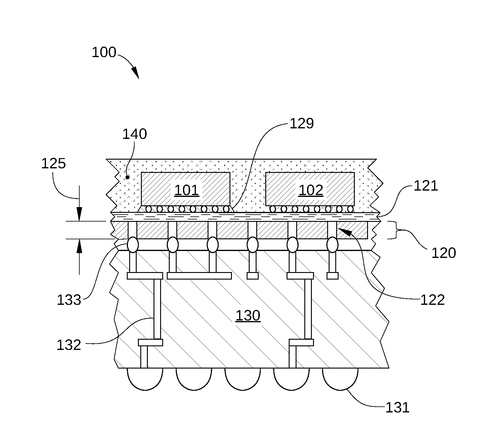
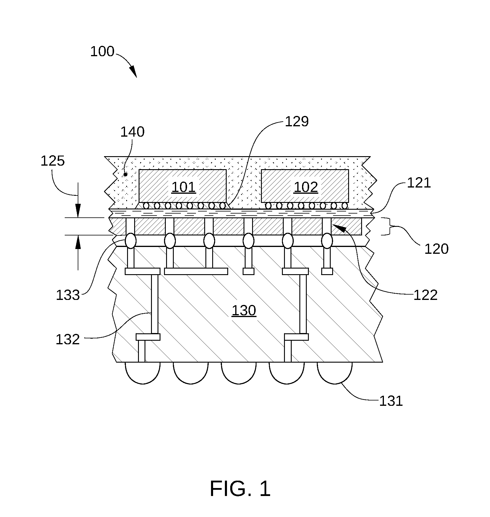
[0017]FIG. 1 is a schematic cross-sectional view of a IC package 100, arranged according to one embodiment of the invention. IC package 100 includes integrated circuit (IC) chips 101 and 102 coupled to an interposer 120, a packaging substrate 130, and an over-molding 140 formed over IC chips 101 and 102. IC package 100 is configured to electrically and mechanically connect IC chips 101, 102, and any other logic or memory ICs coupled to interposer 120 to a printed circuit board or other mounting substrate (not shown) external to IC package 100. In addition, IC package 100 protects IC chips 101 and 102 from ambient moisture and other contamination and minimizes mechanical shock and stress thereon.

[0018]Each of IC chips 101 and 102 may be a semiconductor die singulated from a separately processed semiconductor substrate, such as a central processing unit (CPU), a graphics processing unit (GPU), an application processor or other logic device, a memory chip, a global positioning system (...


PUM


Abstract

An integrated circuit package includes an interposer and an integrated circuit die. The interposer is formed from a layer of semiconductor material that is separated from a bulk portion of a semiconductor substrate, and the integrated circuit die is coupled to the interposer. Vias in the interposer can be formed in the thin layer of semiconductor material removed from the semiconductor substrate, and therefore can be scaled down significantly in size. Such reduced-size, through-interposer vias can be etched and filled much more cost-effectively and result in greatly reduced parasitic capacitance in the integrated circuit package.

Description

BACKGROUND OF THE INVENTION[0001]1. Field of the Invention[0002]Embodiments of the present invention relate generally to integrated circuit chip packaging and, more specifically, to an integrated circuit package with an interposer formed from a reusable carrier substrate.[0003]2. Description of the Related Art[0004]In the packaging of integrated circuit (IC) chips, a key technology is the use of through-silicon vias (TSVs). TSVs are conductive paths formed entirely through an IC chip or silicon interposer, and help enable 3D chip design, which is a packaging design in which multiple IC chips are stacked or placed tightly side by side. In 3D chip design, signals can be transferred directly between chips in a chip package without using exceedingly long interconnect traces or wire bonds, thereby avoiding latency and crosstalk issues in the chip package.[0005]Typically, when TSVs are formed through a silicon interposer, openings are etched into a silicon interposer substrate and filled ...

Claims


Application Information

Patent Timeline
Patent Type & Authority Applications(United States)
IPC IPC(8): H01L23/522H01L21/768
CPCH01L21/76877H01L23/5226H01L23/147H01L23/49816H01L23/5384H01L23/5385H01L2224/83005H01L2224/16225H01L2224/32225H01L2224/73204H01L2224/81005H01L2924/15311H01L21/76898H01L2221/68381H01L2221/68359H01L21/6835H01L2221/68345H01L2221/68377H01L2924/00
Inventor YEE, ABRAHAM F.CHEN, JOHN Y.
Owner NVIDIA CORP
Why Eureka
Try Eureka