Die Seal Ring and Method of Forming the Same

a seal ring and die sealing technology, applied in the direction of semiconductor devices, semiconductor/solid-state device details, electrical devices, etc., can solve the problems of less than 108/b> die seal ring b>108/b>, shrinking device line width, and increasing the complexity of the sealing process, so as to achieve strong protection

Active Publication Date: 2014-12-18
MARLIN SEMICON LTD
View PDF10 Cites 12 Cited by
  • Summary
  • Abstract
  • Description
  • Claims
  • Application Information

AI Technical Summary

Benefits of technology

[0011]The present invention provides a die seal ring and a method of forming the same. The die seal ring includes a first layer in which the layout of thereof has a stamp like structure. In this way, the die seal ring can be more rigid and give a strong protection for the encompassed active region.

Problems solved by technology

With the development of technology and the increasingly imaginative applications of electrical products, the IC device is becoming smaller, more delicate and more diversified.
However, because the line width of the devices are becoming shrinking and width the die seal ring 108 is becoming less as well.

Method used


Image

  • Die Seal Ring and Method of Forming the Same
  • Die Seal Ring and Method of Forming the Same
  • Die Seal Ring and Method of Forming the Same

Examples


Embodiment Construction

[0017]To provide a better understanding of the presented invention, preferred embodiments will be made in detail. The preferred embodiments of the present invention are illustrated in the accompanying drawings with numbered elements.

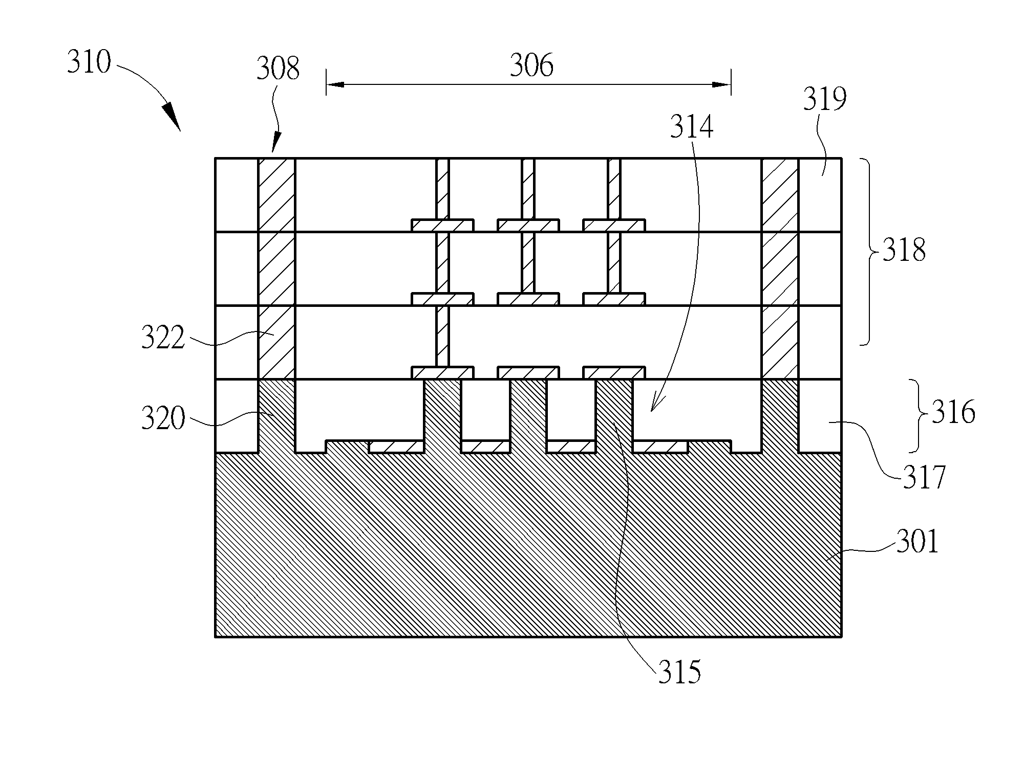
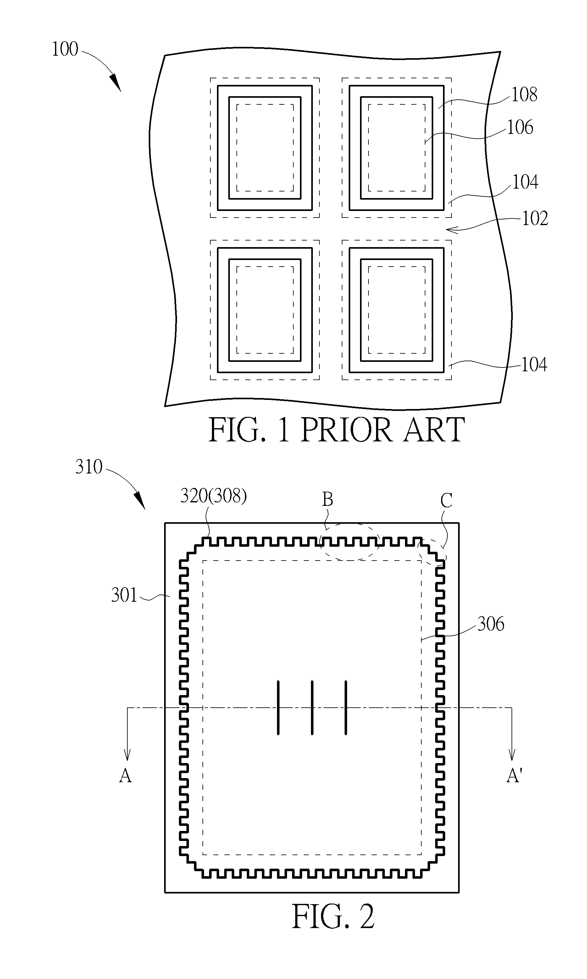
[0018]Please refer to FIG. 2 and FIG. 3, which show schematic diagrams of the die seal ring in a chip according to one embodiment of the present invention, wherein FIG. 3 is a cross-sectional view taken along line AA' in FIG. 2. As shown in FIG. 2, a die seal ring 308 is in a chip 310 and completely encompasses an active region 306. Preferably, the die seal ring 308 is disposed at the most periphery area of the chip 310.

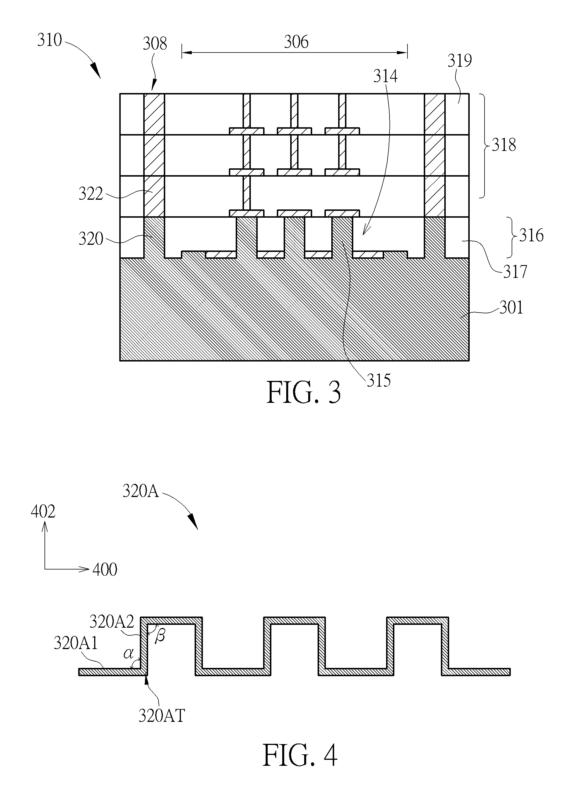
[0019]As shown in FIG. 3, the chip 310 in the present invention includes a substrate 301 and an intra-dielectric (ILD) layer 317, a plurality of inter-metal dielectric (IMD) layers 319 disposed on the substrate 301. In the active region 306, a plurality of active components such as Fin-FET 314 having a fin structure 315 are disposed in th...


PUM


Abstract

A die seal ring is provided. The die seal ring includes a substrate and a first layer extruding from the substrate. The first layer has a first fin ring structure and a layout of the first fin ring structure has a stamp-like shape. In addition, a method for forming a die seal ring is provided. A substrate having an active region is provided. A patterned sacrificial layer is formed on the substrate. A spacer is formed on the sidewall of the patterned sacrificial layer. The patterned sacrificial layer is removed. The substrate is patterned by using the spacer as a mask, thereby simultaneously forming at least a fin structure of a Fin-FET and a first layer of the die seal ring.

Description

BACKGROUND OF THE INVENTION [0001]1. Field of the Invention[0002]The present invention relates to a die seal ring in a chip, and more particularly, to a die seal ring having a stamp structure.[0003]2. Description of the Prior Art[0004]In modern society, the micro-processor system comprised of integrated circuits (IC) is a ubiquitous device, being utilized in such diverse fields as automatic control electronics, mobile communication devices and personal computers. With the development of technology and the increasingly imaginative applications of electrical products, the IC device is becoming smaller, more delicate and more diversified.[0005]As is well known in the art, an IC device is produced from dies that are fabricated by conventional semiconductor manufacturing processes. The process to manufacture a die starts with a wafer: first, different regions are marked on the wafer; second, conventional semiconductor manufacture processes such as deposition, photolithography, etching or...

Claims


Application Information

Patent Timeline
Patent Type & Authority Applications(United States)
IPC IPC(8): H01L23/00H01L21/78H01L21/768
CPCH01L23/562H01L21/78H01L21/76838H01L2924/0002H01L23/585H01L2924/00
Inventor WEI, MING-TETSAO, PO-CHAOYANG, CHING-LICHEN, CHIEN-YANGCHEN, HUI-LINGHUANG, GUAN-KAI
Owner MARLIN SEMICON LTD
Why Eureka
Try Eureka