

Semiconductor device having dll circuit
a technology of dll circuit and semiconductor device, which is applied in the direction of electrical apparatus, push automatic control, etc., can solve the problem of difficult to bring the dll circuit into the lock state within the maximum lock cycle, and achieve the effect of quickly shifting the dll circuit to the lock sta
- Summary
- Abstract
- Description
- Claims
- Application Information
AI Technical Summary
Benefits of technology
Problems solved by technology
Method used
Image

Examples
first embodiment
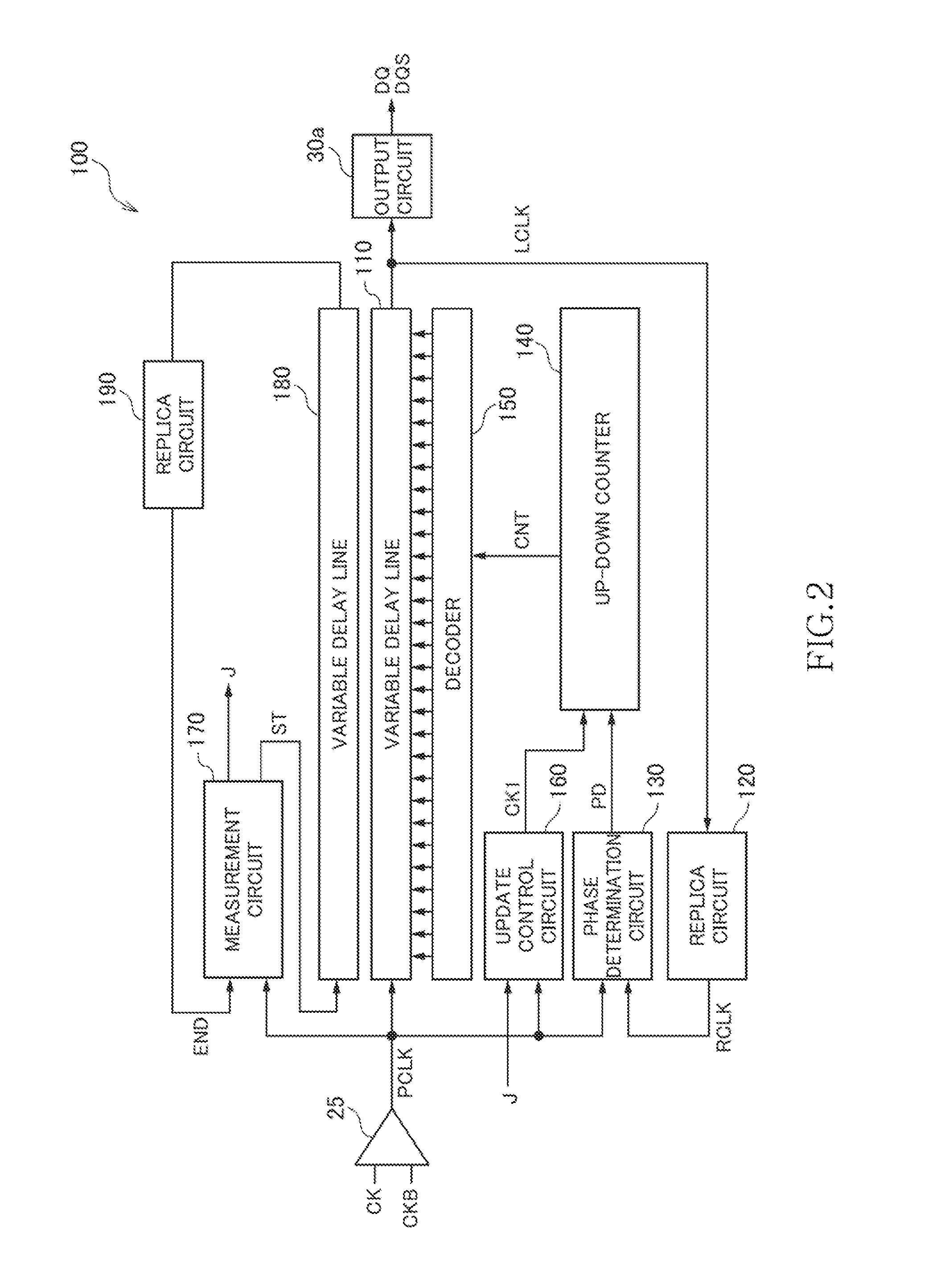
[0039]Although not particularly limited thereto, in the first embodiment, when the phase A of the replica clock signal RCLK passes over the target TG three times, the DLL circuit 100 is determined to be in the lock state. That is, when the up-down counter 140 performs an operation in the order of counting up, counting down, and counting up, or performs an operation in the order of counting down, counting up, and counting down, the DLL circuit 100 is determined to be in the lock state.
[0040]In the example shown in FIG. 3, because the generation interval of the update signal CK1 is appropriate, the DLL circuit 100 is shifted to the lock state relatively early. However, when the generation interval of the update signal CK1 is constant, it may take a long time to shift the DLL circuit 100 to the lock state depending on the frequency of the clock signal CK or the length of the delay time tDL. For example, when the generation interval of the update signal CK1 is too long relative to the d...
second embodiment
[0063]the present invention is explained next.
[0064]Turning to FIG. 8, the DLL circuit 100a according to the second embodiment is different from the DLL circuit 100 shown in FIG. 2 in that an update control circuit 210 is used instead of the update control circuit 160, and a count-value determination circuit 220 is added. The measurement circuit 170, the variable delay line 180, and the replica circuit 190 are omitted from the DLL circuit 100a. Other features of the DLL circuit 100a are identical to those of the DLL circuit 100 shown in FIG. 2, and thus like reference numerals are denoted to like elements and redundant explanations thereof will be omitted.
[0065]Instead of the count value J, a selection signal SEL is supplied to the update control circuit 210 from the count-value determination circuit 220. The count-value determination circuit 220 receives the count value CNT of the up-down counter 140, and controls a logic level of the selection signal SEL depending on whether the c...
third embodiment
[0073]the present invention is explained next.
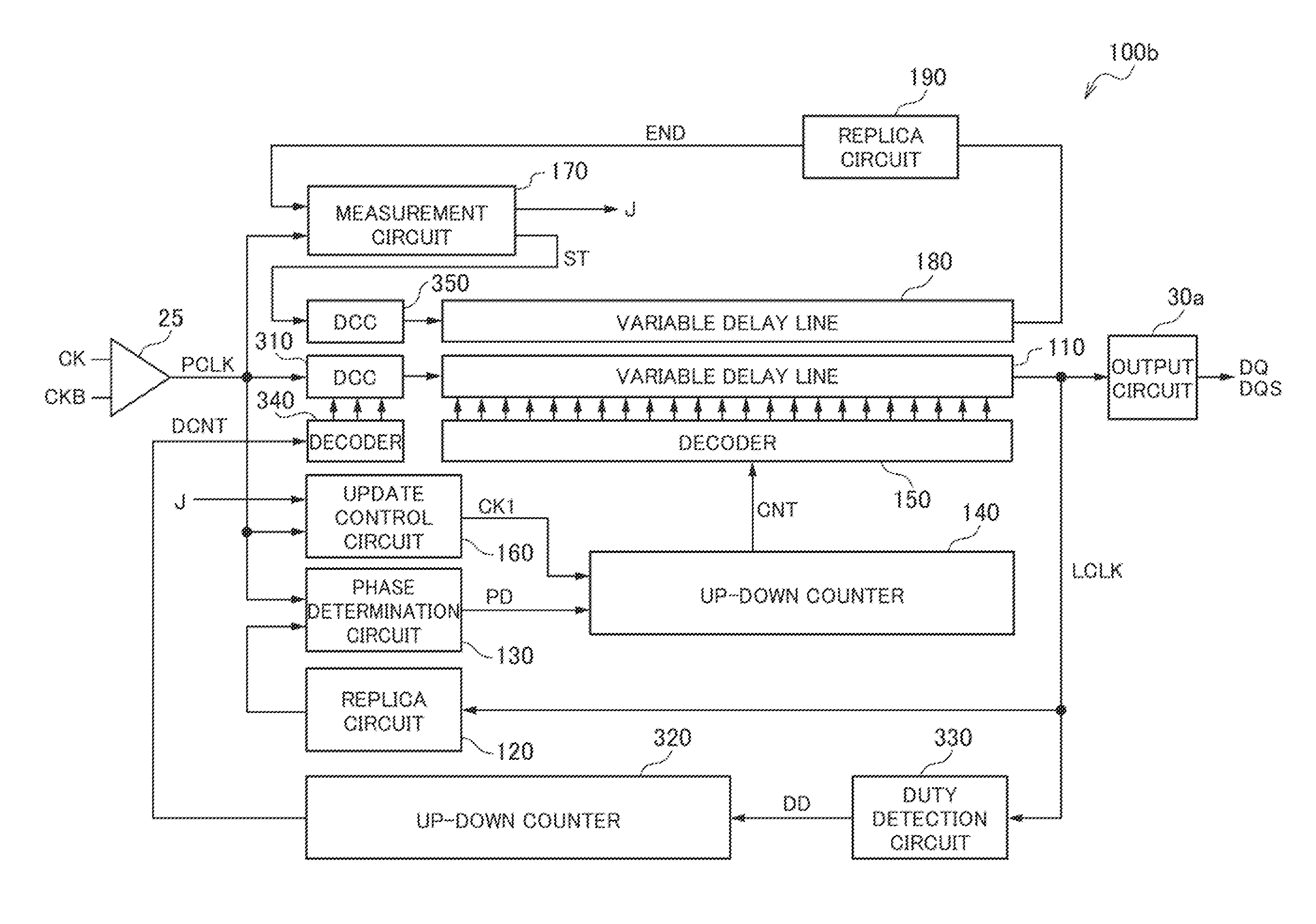
[0074]Turning to FIG. 11, the DLL circuit 100b according to the third embodiment is different from the DLL circuit 100 shown in FIG. 2 in that a duty correction circuit (DCC) 310 is inserted at the previous stage of the variable delay line 110. The duty correction circuit 310 is a circuit that adjusts the duty ratio of the internal clock signal PCLK. The adjustment of the duty ratio is controlled based on an output of a decoder 340 that decodes a count value DCNT of an up-down counter 320. The count value of the up-down counter 320 is counted up or counted down according to an output signal DD of a duty detection circuit 330 that detects the duty ratio of the internal clock signal LCLK. Therefore, the duty correction circuit 310 adjusts the duty ratio of the internal clock signal PCLK so as to become 50%.
[0075]In the DLL circuit 100b configured as described above, a loop delay of a duty-adjusting feedback loop is sometimes greater than t...
PUM
 Abstract
Description
Claims
Application Information