

Window for display device and display device including the window panel
a display device and window panel technology, applied in the field of windows for display devices and display devices, can solve the problems of deformation of the window, easy damage of the window, plastic substrates, etc., and achieve the effect of satisfying optical properties and excellent reliability
- Summary
- Abstract
- Description
- Claims
- Application Information
AI Technical Summary
Benefits of technology
Problems solved by technology
Method used
Image

Examples
example 1
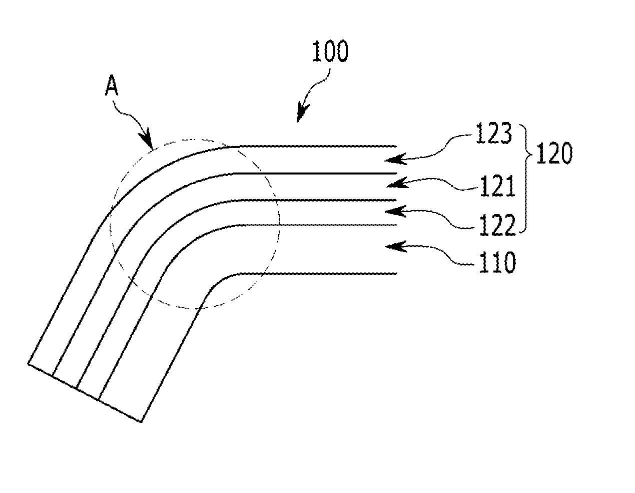
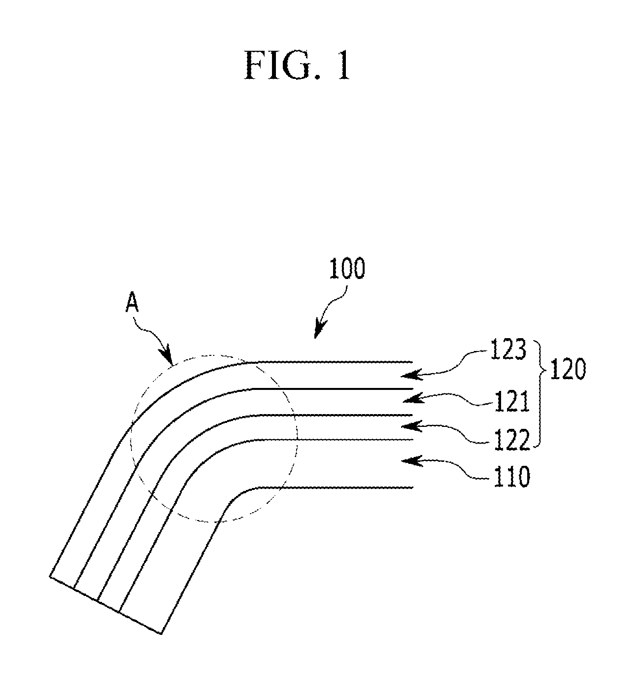
[0067]A window for a display device having a polymer resin layer, a first plastic substrate, a second plastic substrate, a buffer layer, and a hard coating layer as provided in the following Table 1 was manufactured in an IML (In Mold Labeling) injection method.
TABLE 1MaterialThicknessPolymer resin layerPolycarbonate (PC)700 μm First plastic substrateUpper plate:15 μmpolymethylmethacrylate (PMMA)Rear plate:60 μmpolycarbonate (PC)Buffer layerOCA50 μmSecond plasticPolymethylmethacrylate (PMMA)200 μm substrateHard coating layerAcryl-based resin30 μm
example 2
[0068]A window for a display device having a polymer resin layer, a first plastic substrate, a second plastic substrate, a buffer layer, and a hard coating layer as provided in the following Table 2 was manufactured in an IML (In Mold Labeling) injection method.
TABLE 2MaterialThicknessPolymer resin layerPolymethylmethacrylate (PMMA)700 μmFirst plastic substratePolymethylmethacrylate (PMMA)100 μmBuffer layerOCA 50 μmSecond plasticPolymethylmethacrylate (PMMA)200 μmsubstrateHard coating layerAcryl-based resin 30 μm
example 3
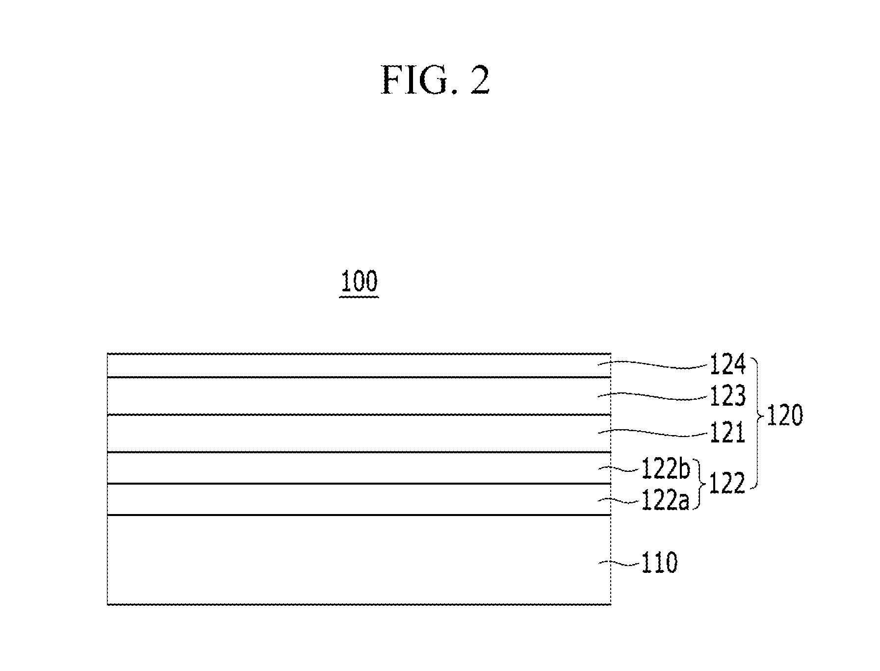
[0069]A window for a display device having a polymer resin layer, a first plastic substrate, a second plastic substrate, a buffer layer, a hard coating layer, and a binder layer as provided in the following Table 3 was manufactured in an IML (In Mold Labeling) method.
TABLE 3MaterialThicknessPolymer resin layerPolycarbonate (PC)700 μmBinder layerPolyester 20 μmFirst plastic substratePolymethylmethacrylate (PMMA)100 μmBuffer layerOCA 50 μmSecond plasticPolymethylmethacrylate (PMMA)150 μmsubstrateHard coating layerAcryl-based resin 30 μm
PUM
| Property | Measurement | Unit |
|---|---|---|
| Thickness | aaaaa | aaaaa |
| Thickness | aaaaa | aaaaa |
| Thickness | aaaaa | aaaaa |
Abstract
Description
Claims
Application Information