Low Temperature Salicide for Replacement Gate Nanowires

Inactive Publication Date: 2015-01-22
ALSEPHINA INNOVATIONS INC
View PDF3 Cites 15 Cited by
  • Summary
  • Abstract
  • Description
  • Claims
  • Application Information

AI Technical Summary

Benefits of technology

The present invention provides techniques for integrating low temperature salicide formation in a replacement gate device process flow. This allows for the fabrication of field-effect transistor (FET) devices with improved performance and reliability. The method includes the formation of a dummy gate, removal of the dummy gate to form a trench, deposition of a replacement gate, annealing of the replacement gate, and the formation of a gate cap and salicide on the exposed source and drain regions of the device. The invention provides for improved device performance and reliability.

Problems solved by technology

While a high temperature compatible material will permit the formation of a self-aligned silicide (a salicide), desirable metals such as nickel cannot be used.
Alignment issues are prevalent with a trench silicide scheme, especially when dealing with scaled device dimensions.

Method used


Image

  • Low Temperature Salicide for Replacement Gate Nanowires
  • Low Temperature Salicide for Replacement Gate Nanowires
  • Low Temperature Salicide for Replacement Gate Nanowires

Examples


Embodiment Construction

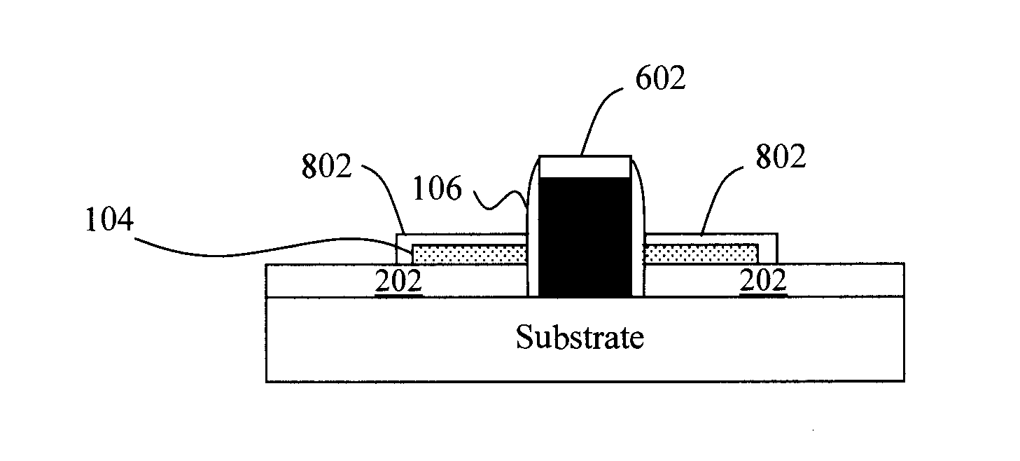
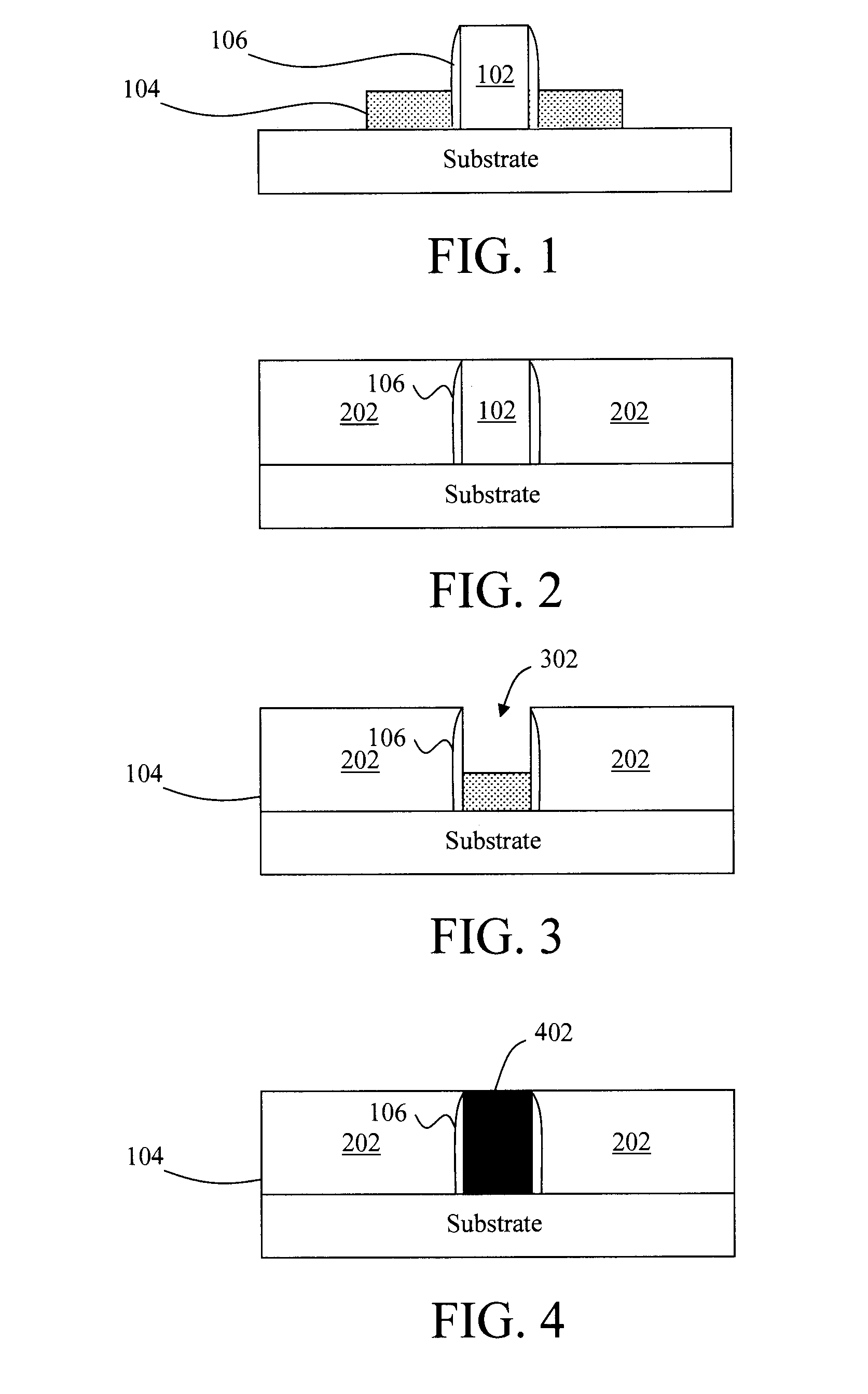
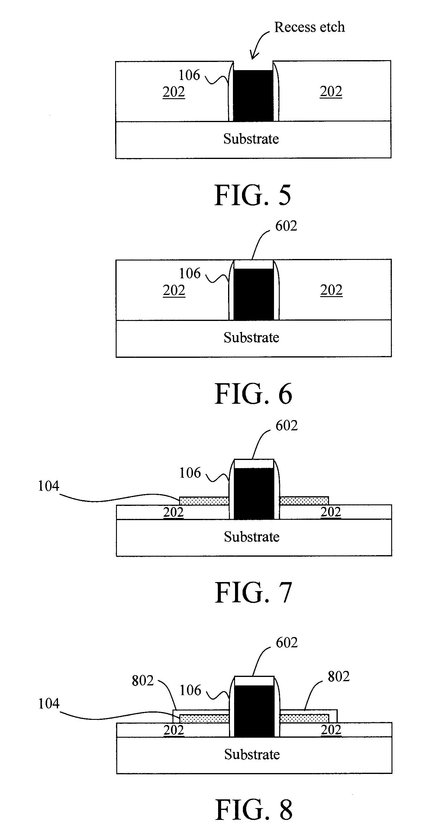
[0028]Provided herein are techniques that enable the use of a low temperature salicide in a replacement gate process flow. The term “low temperature salicide” as used herein refers to a self-aligned silicide (i.e., a salicide) that would be degraded by exposure to the high temperatures encountered with the replacement gate process during the final gate anneal. As will be described in detail below, the present process involves de-layering the gap-fill dielectric after the replacement gate formation, which permits the low temperature salicide to be formed after the replacement gate anneal.

[0029]An overview of the present techniques is first provided by way of reference to FIGS. 1-8, followed by an exemplary implementation in the context of a fin first, wire last, gate-all-around (GAA) device shown illustrated in FIGS. 9-19. The present techniques are generally applicable to any replacement gate device fabrication process, including but not limited to, FinFET, nanowire and planar devic...


PUM


Abstract

Techniques for integrating low temperature salicide formation in a replacement gate device process flow are provided. In one aspect, a method of fabricating a FET device is provided that includes the following steps. A dummy gate(s) is formed over an active area of a wafer. A gap filler material is deposited around the dummy gate. The dummy gate is removed selective to the gap filler material, forming a trench in the gap filler material. A replacement gate is formed in the trench in the gap filler material. The replacement gate is recessed below a surface of the gap filler material. A gate cap is formed in the recess above the replacement gate. The gap filler material is etched back to expose at least a portion of the source and drain regions of the device. A salicide is formed on source and drain regions of the device.

Description

FIELD OF THE INVENTION[0001]The present invention relates to replacement gate fabrication processes and more particularly, to techniques for integrating low temperature salicide formation in a replacement gate device process flow.BACKGROUND OF THE INVENTION[0002]A gate-last CMOS fabrication process is often used for material availability and stress-induced performance enhancement reasons. Also called a replacement-gate process, the gate-last approach generally requires a high temperature anneal after the gate dielectric is deposited in order to improve reliability of the dielectric.[0003]Thus every component of the device that is present prior to the anneal must be compatible with high processing temperatures. One aspect of the device design particularly impacted by this requirement is the silicidation process commonly employed to form source and drain contacts. In this regard, with conventional device fabrication techniques, the use of a replacement gate process forces the device d...

Claims


Application Information

Patent Timeline
IPC IPC(8): H01L29/78H01L29/66
CPCH01L29/78H01L29/665H01L21/823431B82Y10/00B82Y40/00H01L21/845H01L29/0665H01L29/0669H01L29/0673H01L29/66439H01L29/66545H01L29/66795H01L29/775H01L29/785H01L29/41775
Inventor CHANG, JOSEPHINE B.GUILLORN, MICHAEL A.LAUER, GEN P.LAUER, ISAACSLEIGHT, JEFFREY W.
Owner ALSEPHINA INNOVATIONS INC
Why Eureka
Try Eureka