Package structure of optical module
- Summary
- Abstract
- Description
- Claims
- Application Information
AI Technical Summary
Benefits of technology
Problems solved by technology
Method used
Image
Examples
Embodiment Construction
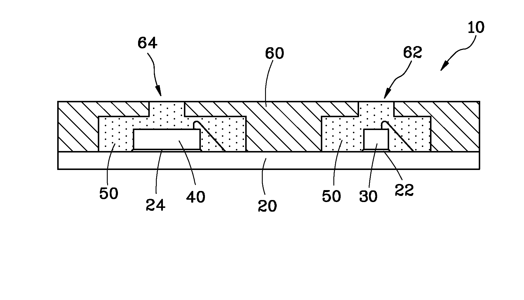
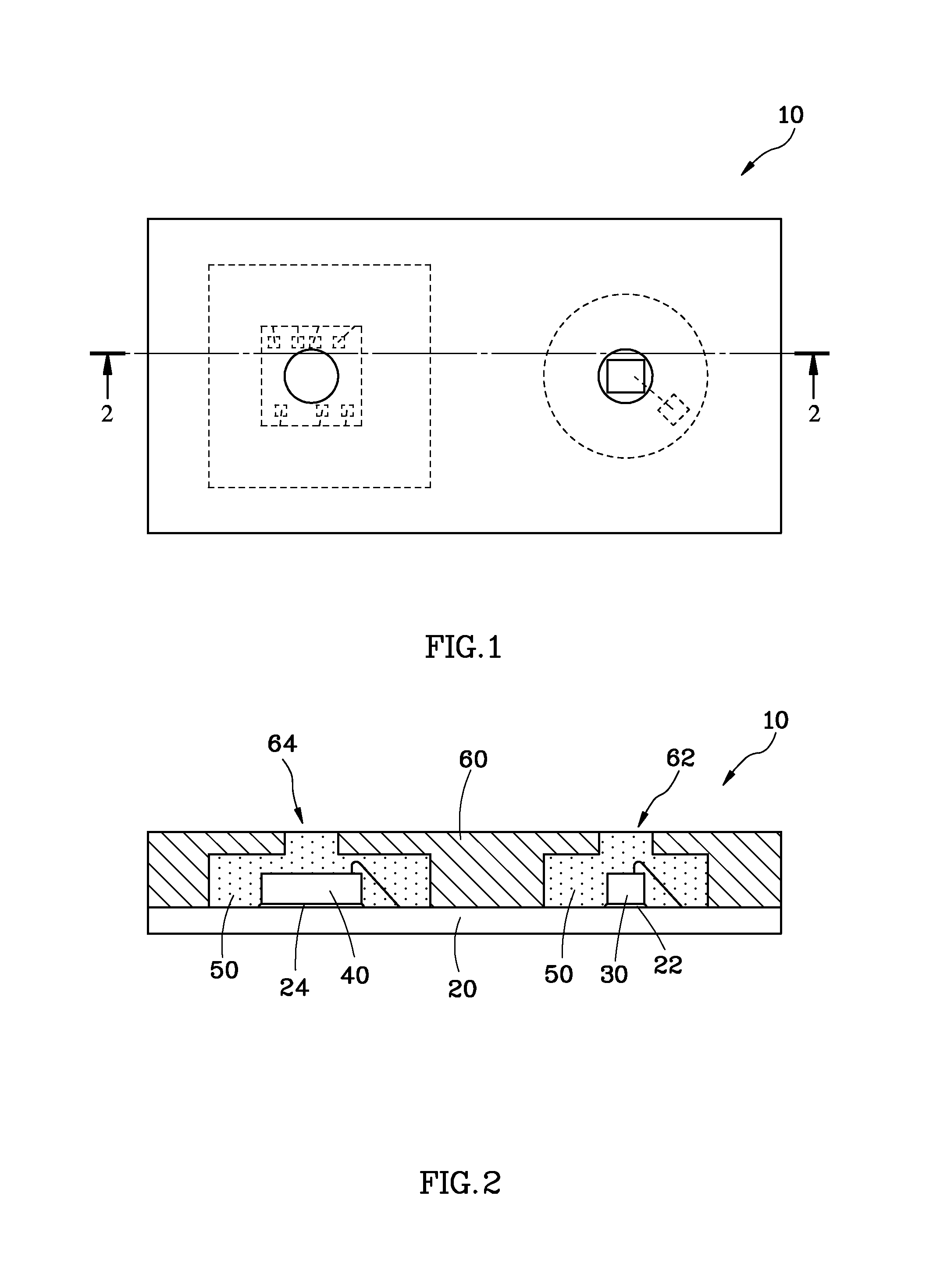
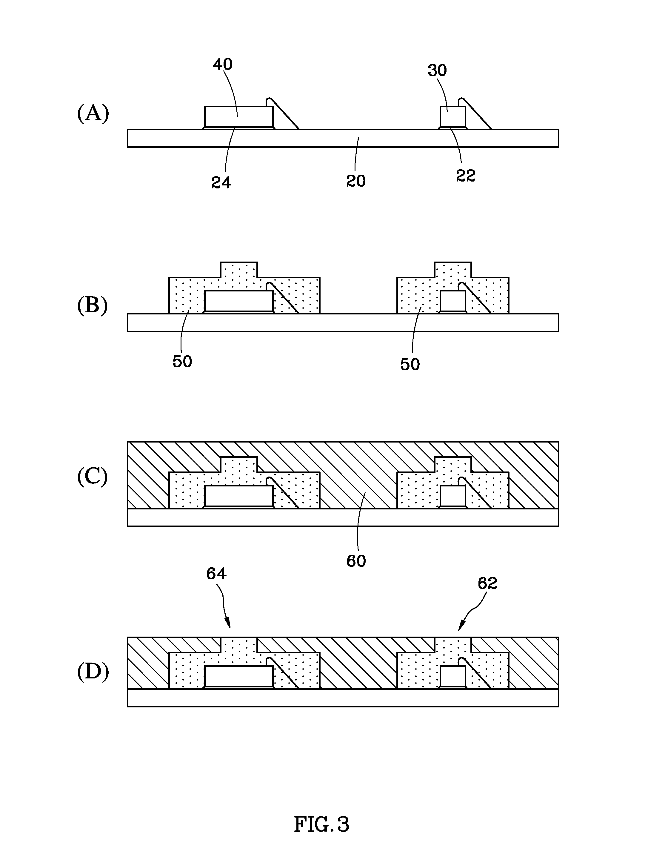
[0032]Referring to FIG. 1 through FIG. 2, an optical module package structure 10 provided according to a preferred embodiment of the present invention results from cutting a module from a typical package array and comprises a substrate 20, a light-emitting chip 30, a light-admitting chip 40, two encapsulants 50, and a shielding layer 60.
[0033]The substrate 20 is a non-ceramic substrate made of an organic material, such as Bismaleimide Triazine, and thus the substrate 20 incurs a low material cost. The substrate 20 is defined with a light-emitting region 22 and a light-admitting region 24.
[0034]The light-emitting chip 30 and the light-admitting chip 40 undergo a die attaching process and a wire bonding process so as to be disposed at the light-emitting region 22 and the light-admitting region 24 of the substrate 20, respectively. The light-emitting chip 30 emits the light beam. The light-admitting chip 40 receives the light beam emitted from the light-emitting chip 30.
[0035]The encap...
PUM
 Abstract
Description
Claims
Application Information
 - R&D Engineer
- R&D Manager
- IP Professional
- Industry Leading Data Capabilities
- Powerful AI technology
- Patent DNA Extraction
Browse by: Latest US Patents, China's latest patents, Technical Efficacy Thesaurus, Application Domain, Technology Topic, Popular Technical Reports.
© 2024 PatSnap. All rights reserved.Legal|Privacy policy|Modern Slavery Act Transparency Statement|Sitemap|About US| Contact US: help@patsnap.com


