Array Substrate and Liquid Crystal Display Panel

a liquid crystal display and substrate technology, applied in the field of array substrates and liquid crystal display panels, can solve the problems of reducing the opening ratio reducing the display brightness in the 2d display mode, and not achieving the effect of lcs, so as to reduce the number of data lines, reduce the number of data drivers, and reduce the cost

Inactive Publication Date: 2015-02-05
TCL CHINA STAR OPTOELECTRONICS TECH CO LTD
View PDF6 Cites 9 Cited by
  • Summary
  • Abstract
  • Description
  • Claims
  • Application Information

AI Technical Summary

Benefits of technology

[0026]The benefits of the present invention are as follows. Differing from the situation of the prior art, in the array substrate according to the present invention, each pixel unit utilizes one first scanning line, one second scanning line, one third scanning line and one data line to drive. Comparing to the prior art, it reduces the number of data lines, and further accordingly reduces the number of data drivers, which is conducive to reduce the cost. Additionally, each pixel unit comprises a first control circuit and a second control circuit. The first control circuit affects the first pixel electrode when the second scanning line inputs the second scanning signal, so that the first pixel electrode is under the state of displaying the image corresponding to the black screen. The second control circuit affects the second pixel electrode and the third pixel electrode when the third scanning line inputs the third scanning signal, which changes the voltage difference between the second pixel electrode and the third pixel electrode. In the 2D display mode, the second scanning line controls the first control circuit, so that the first control circuit control the first pixel electrode under the state of correspondingly displaying the voltage of 2D screen, and then the first pixel electrode in the 2D display mode is under the state of displaying the image corresponding to the 2D screen. That is, the first pixel electrode, the second pixel electrode and the third pixel electrode are under the state of displaying the image corresponding to the 2D screen. Therefore, it improves the opening ratio, and the third scanning line controls the second control circuit, so that the second control circuit affects the second pixel electrode and the third pixel electrode, and there are voltage differences which are not zero within the first pixel electrode, the second pixel electrode and the third pixel electrode. Thereby, it can reduce the color difference in wide viewing angle in the 2D display mode. In the 3D display mode, the second scanning line controls the first control circuit to affect the first pixel electrode, so that the first pixel electrode is under the state of displaying the image corresponding to black screen. The first electrode under the state of displaying the image corresponding to black screen can block the wrong left-eye image and wrong right-eye image. Therefore, it can reduce the 3D eyes signal crosstalk. The third scanning line controls the second control circuit to affect the second pixel electrode and the third pixel electrode, which changes the voltage difference between the second pixel electrode and the third pixel electrode, so that there is voltage difference which is not zero between the second pixel electrode and the third pixel electrode. Thereby, it can reduce the color difference in wide viewing angle in the 3D display mode.

Problems solved by technology

However, the left-eye and right-eye images are easy to occur crosstalk, which causes the observer to see overlapping images, affecting the viewing experience.
However, this way will result the reduction of the opening ratio in the 2D display mode and lower the display brightness in the 2D display mode.
However, in 3D display mode, because the main pixel region displays the dark screen, there is only one sub pixel region normally displaying 3D image in the 3D display mode, which can not achieve the effect of LCS and the color distortion in wide angle can still be observed.
However, in the above technical solution, each pixel needs two data lines to drive, which correspondingly increases the number of data drivers and is not conducive to cost reduction.

Method used


Image

  • Array Substrate and Liquid Crystal Display Panel
  • Array Substrate and Liquid Crystal Display Panel
  • Array Substrate and Liquid Crystal Display Panel

Examples


Embodiment Construction

[0034]The detailed descriptions accompanying drawings and the embodiment of the present invention are as follows,

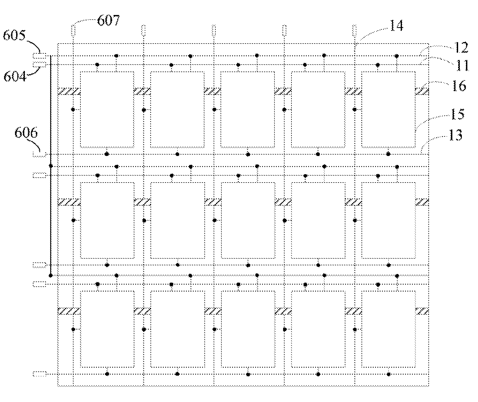
[0035]Referring to FIGS. 3 to 5, in the array substrate according to an embodiment of the present invention, the array substrate comprises multiple first scanning lines 11, multiple second scanning lines 12, multiple third scanning lines 13, multiple data lines 14, and multiple pixel units 15 arranged in rows. The array substrate further comprises a common electrode 16 used to input common voltage. Each pixel unit 15 corresponds to one first scanning line 11, one second scanning line 12, one third scanning line 13 and one data line 14.

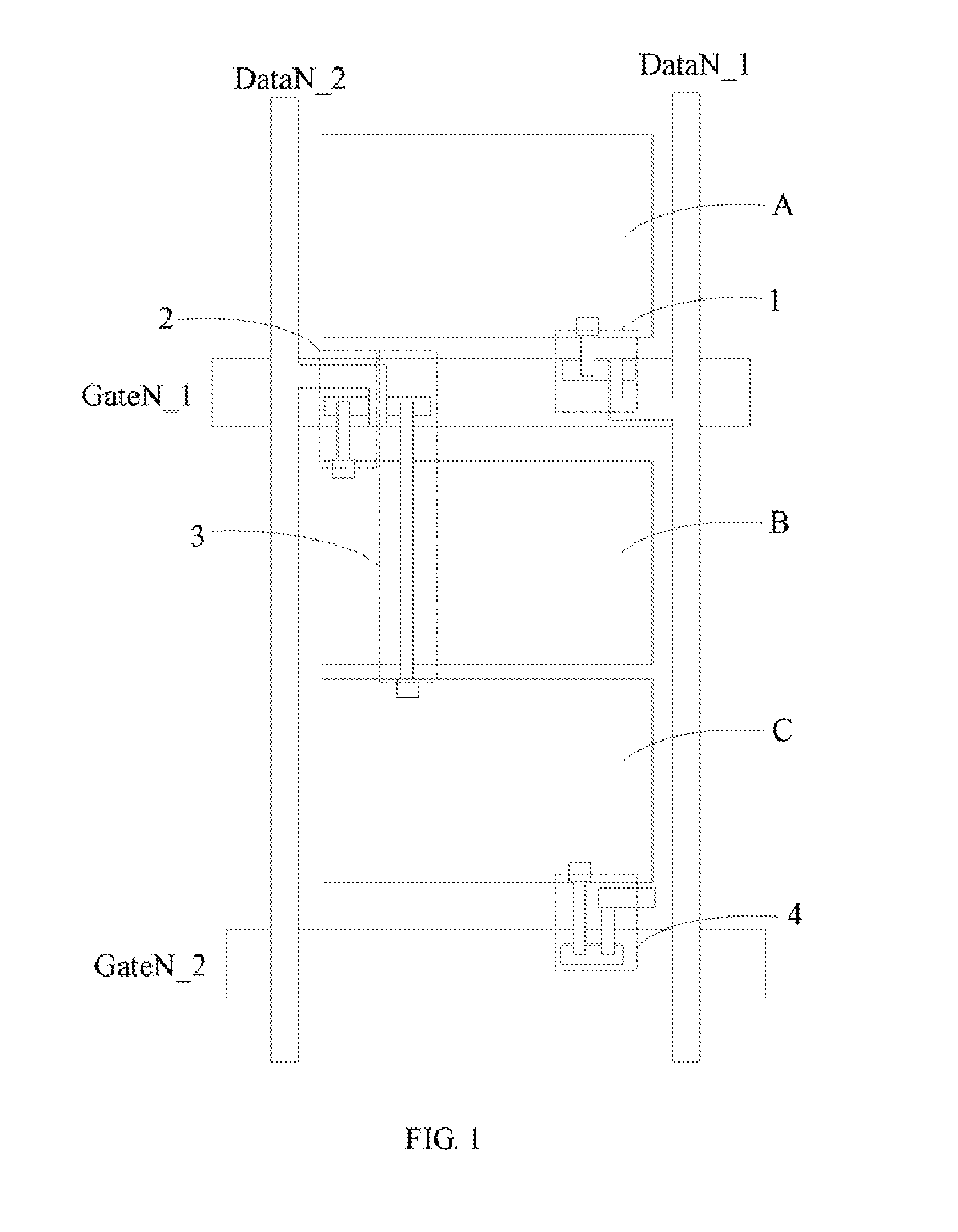
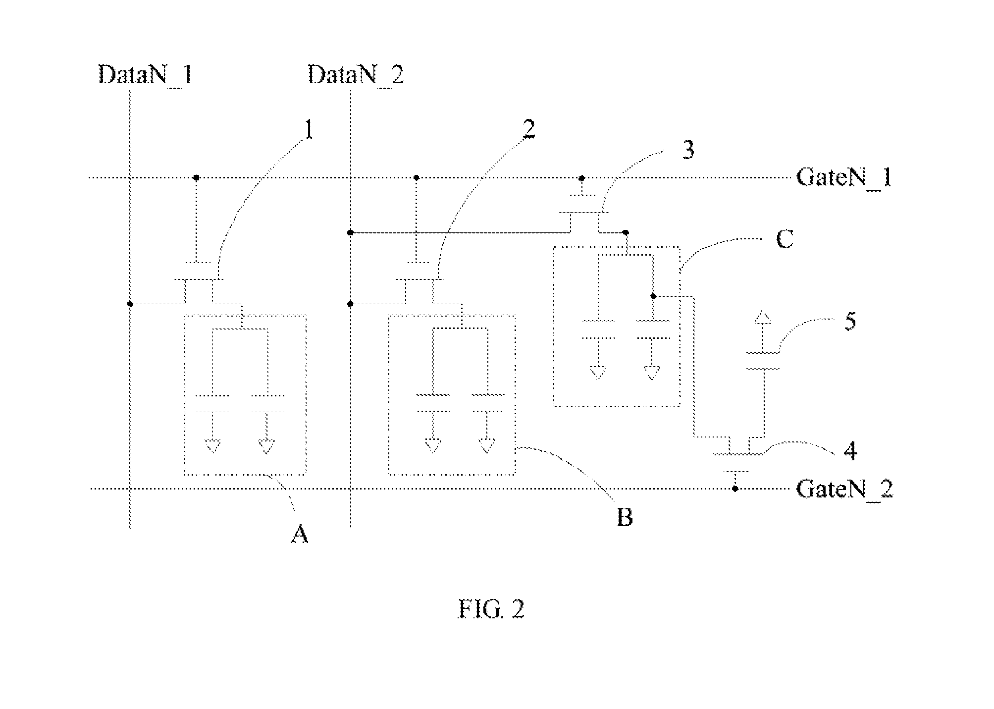
[0036]Wherein, referring to FIG. 5, each pixel unit 15 comprises a first pixel electrode M1, a second pixel electrode M2, a third pixel electrode M3, and a first switch Q1, a second switch Q2 and a third switch Q3 which respectively affect the first pixel electrode M1, the second pixel electrode M2 and the third pixel electrode M3. The contr...


PUM

PropertyMeasurementUnit
voltageaaaaaaaaaa
timeaaaaaaaaaa
voltageaaaaaaaaaa

Abstract

The present invention provides an array substrate and a liquid crystal display panel. Wherein, in the array substrate, each pixel unit comprises a first pixel electrode, a second pixel electrode, and a third pixel electrode. And each pixel unit comprises a first control circuit and a second control circuit. The first control circuit affects the first pixel electrode, so that the first pixel electrode is under the state of displaying the image corresponding to the black screen in the 3D display mode. The second control circuit affects the second pixel electrode and the third pixel electrode to change the voltage difference between the second pixel electrode and the third pixel electrode. By the above way, the present invention can minimize the color difference in wide viewing angle, improve the opening ratio in the 2D display mode, and reduce the crosstalk of the two eyes signal in the 3D display mode. Furthermore, it can reduce the amount of the data drivers and reduce the costs.

Description

BACKGROUND OF THE INVENTION[0001]1. Field of the Invention[0002]The present invention relates to the field of liquid crystal display techniques, and in particular to an array substrate and a liquid crystal display panel.[0003]2. The Related Arts[0004]VA (Vertical Alignment) liquid crystal display panel has the advantages of fast response, high contrast ratio, etc., which is the mainstream development of the present liquid crystal display panel. However, in the different perspective, the alignment direction of the liquid crystal molecules is different, which also makes the effective refractive index of the liquid crystal molecules different. Therefore, it causes the changes of transmitted light intensity. The concrete manifestation is reduction of transmittance ability in oblique angle. The colors in the directions of the oblique angle and the center angle are different, causing the color difference. Therefore, it can be observed the color distortion in wide angle. In order to improv...

Claims


Application Information

Patent Timeline
Patent Type & Authority Applications(United States)
IPC IPC(8): G02F1/133H01L27/12G02F1/1343G02F1/1362G02F1/1368
CPCG02F1/13306G02F1/136213G02F1/1368G02F1/136286G02F2001/136222G02F1/13439H01L27/124H01L27/1255G02F1/136209G09G3/36H04N13/356H04N13/31H04N13/398G02F1/136222
Inventor XUE, JINGFENGHSU, JE-HAOYAO, XIAOHUI
Owner TCL CHINA STAR OPTOELECTRONICS TECH CO LTD
Why Eureka
Try Eureka