Method of manufacturing a component

a manufacturing method and component technology, applied in the direction of manufacturing tools, manufacturing apparatus, transportation and packaging, etc., can solve the problems of unsuitable selection of process parameters, defects may be caused, and defects in final components, and achieve the effect of smaller defects and higher resolution

Active Publication Date: 2015-02-05
ROLLS ROYCE PLC
View PDF6 Cites 81 Cited by
  • Summary
  • Abstract
  • Description
  • Claims
  • Application Information

AI Technical Summary

Benefits of technology

[0035]The intensity of the second electron beam may be lower than the intensity of the first electron beam. Providing the second electron beam as lower intensity beam (for example a beam with a narrower energy distribution profile and / or lower maximum intensity) may allow a higher resolution scan of the solid layer, and thus may allow smaller defects to be identified.

Problems solved by technology

Manufacturing components using EBM has many advantages, including the possibility to manufacture complex 3D shapes with little or no bespoke tooling, but the final components can have defects.
Additionally or alternatively, defects may be caused by unsuitable selection of process parameters, such as inappropriate rastering speed.
Such defects may result in undesirable properties, and may limit the use of the finished components to certain applications and / or necessitate further processing steps (such as hot isostatic pressing, or HIP) to remove the defects in order for the components to have the required properties for a given application.
Thus, the power of the first electron beam may be sufficient to perform selective melting of the powder layer, but the power of the second electron beam may be insufficient to perform selective melting of the powder layer.
This may result in a particularly compact and / or low cost additive layer manufacturing machine.
Such a decision may result in a defect being removed by re-melting using the first electron beam, as described above and elsewhere herein.
The decision may result in no action being taken, for example if a defect is deemed to be within an acceptable tolerance.

Method used


Image

  • Method of manufacturing a component
  • Method of manufacturing a component
  • Method of manufacturing a component

Examples


Embodiment Construction

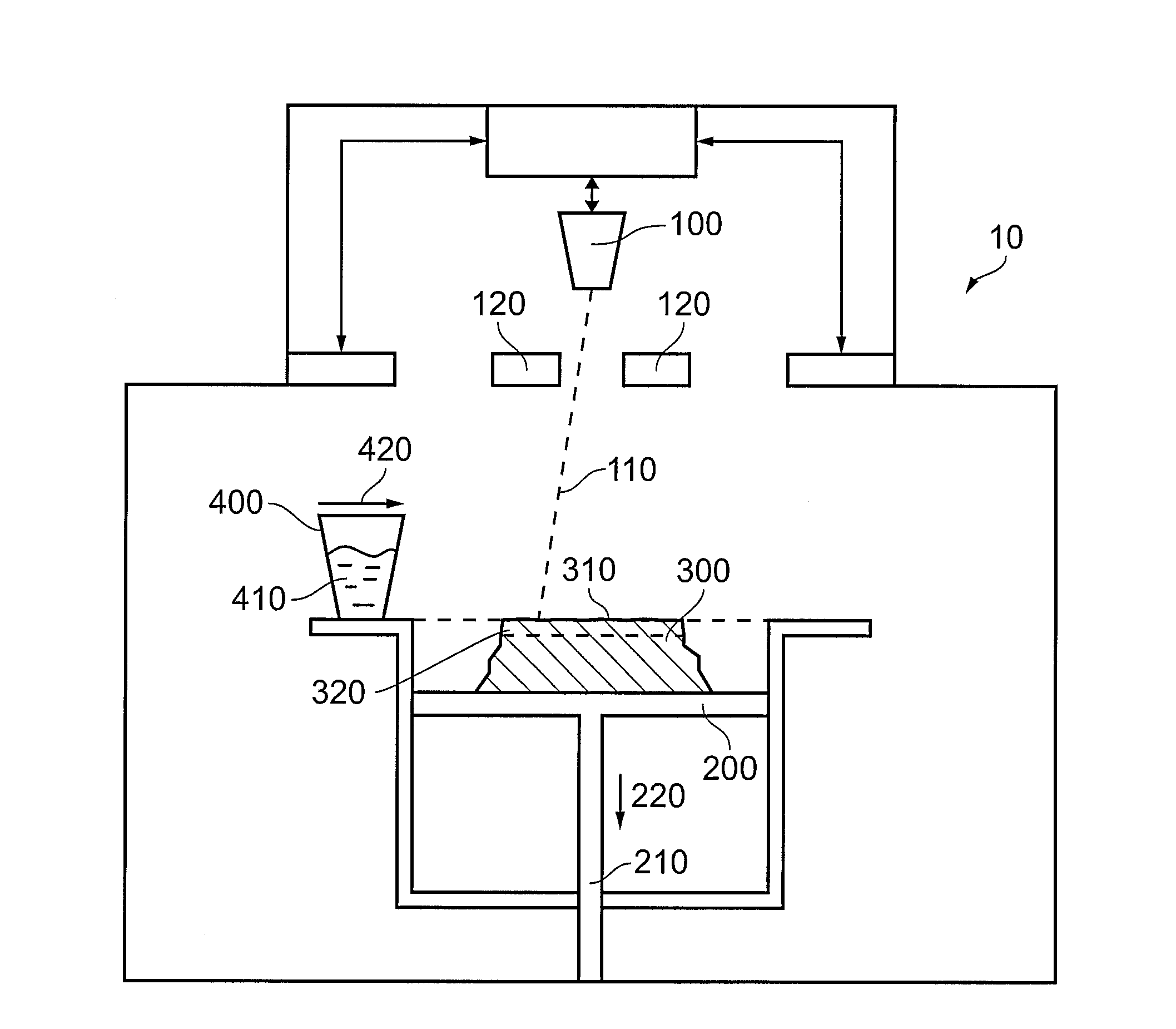
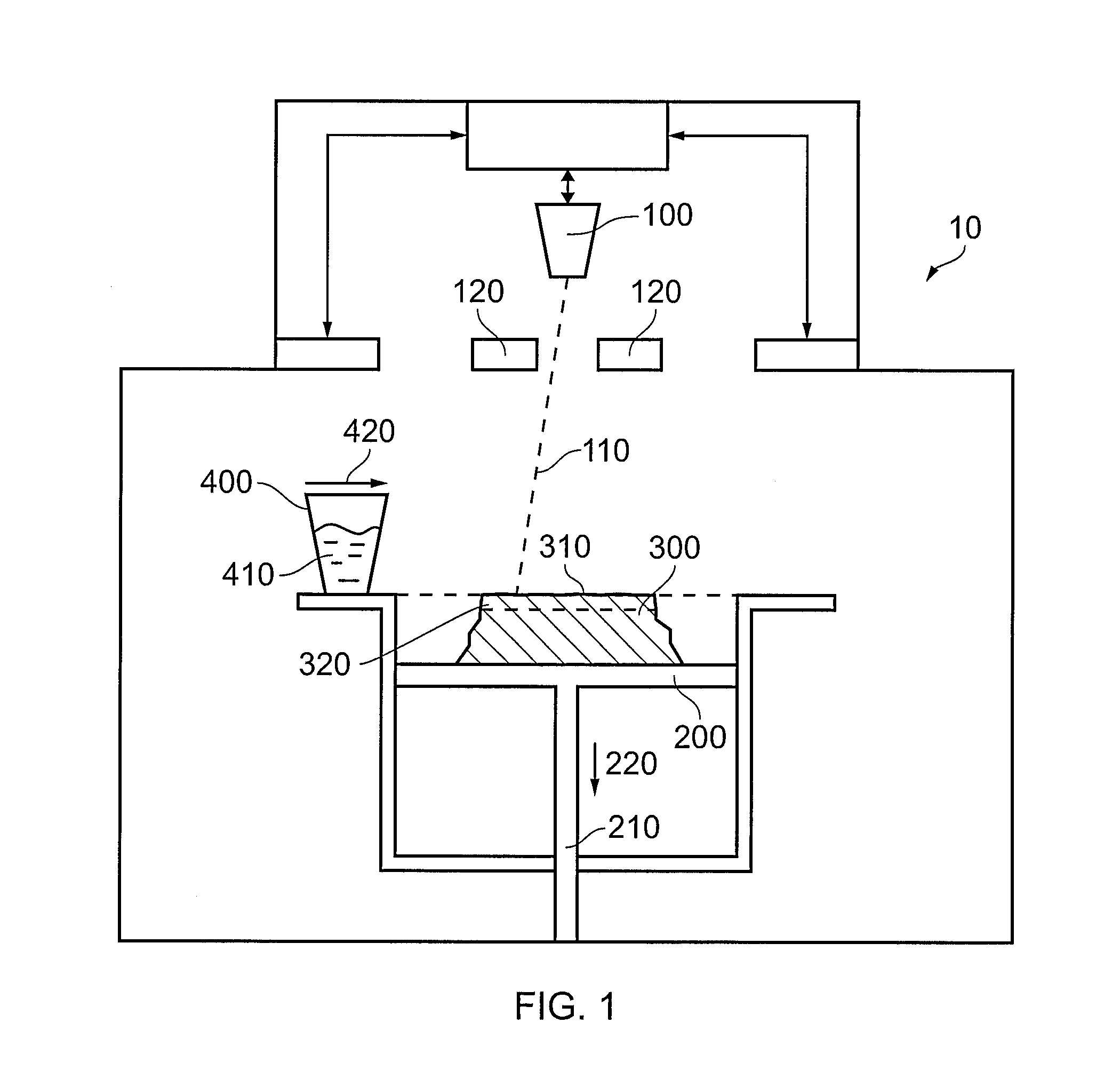
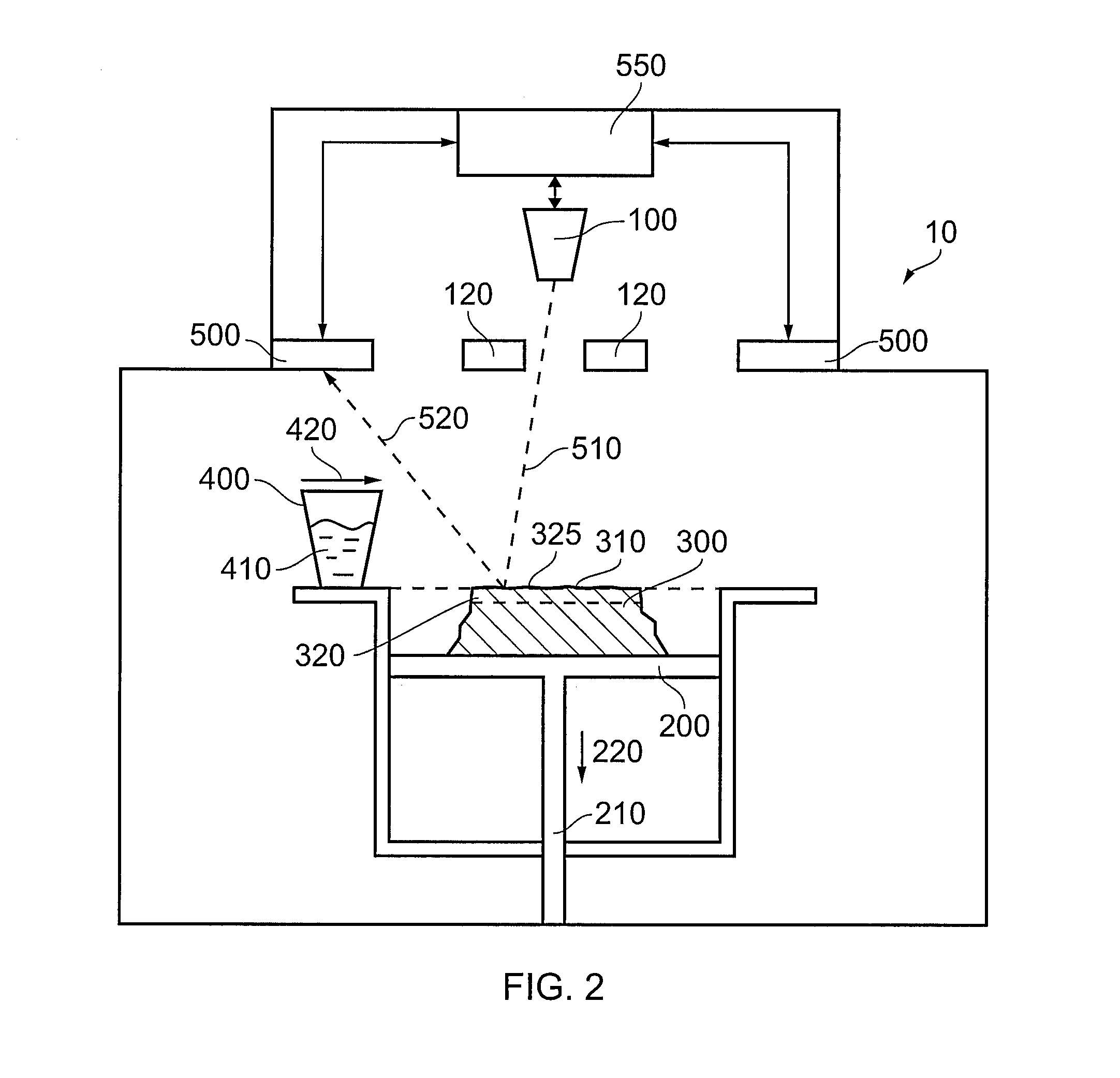
[0042]As explained elsewhere herein, additive layer manufacturing (ALM) methods using electron beam melting (EBM) may be used to manufacture metallic components by sequential selective melting of thin powder layers.

[0043]An example of an additive layer manufacturing machine (or ALM machine) 10 for use in such a method is shown in FIG. 1. The ALM machine 10 comprises an electron beam source 100 for generating an electron beam 110 (which may be referred to as a first electron beam herein). In use, the electron beam 110 is focussed (and optionally split into multiple beams) using focusing elements 120, such as lenses and / or mirrors, towards a component 300 being manufactured. Specifically, the electron beam 110 is focussed onto a layer of powder (for example a layer of powder metal) 310 to be melted by the electron beam which subsequently solidifies to form a solid layer (for example a solid metal layer) of the component 300. The interior of the ALM machine 10, or at least the part of ...


PUM

PropertyMeasurementUnit
thicknessaaaaaaaaaa
poweraaaaaaaaaa
defectsaaaaaaaaaa

Abstract

An additive layer manufacture (ALM) machine generates a first electron beam for selectively melting a layer of metal powder, and a second electron beam for detecting defects in the selectively melted layer once it has solidified. The second electron beam has a lower power than the first electron beam so as to be used to identify any defects without performing further melting. If any defects are detected, they can be removed, for example by re-melting, before the next layer of powder is supplied. The process may be repeated to generate a finished component with good mechanical properties.

Description

CROSS-REFERENCE TO RELATED APPLICATIONS[0001]This application is based upon and claims the benefit of priority from British Patent Application Number 1313840.9 filed 2 Aug. 2013, the entire contents of which is incorporated by reference.BACKGROUND OF THE INVENTION[0002]1. Field of the Disclosure[0003]The present invention relates to a method of manufacturing a component. In particular, the present invention relates to manufacturing a component using additive layer manufacture.[0004]2. Description of the Related Art[0005]Additive layer manufacturing (ALM) methods using electron beam melting (EBM) may be used to manufacture metallic components by sequential selective melting of thin metal powder layers. According to such a method, a layer of metal powder is deposited onto a surface (or plate), and an electron beam is used to selectively melt the powder layer. The melted material then solidifies so as to form a metallic layer of the desired shape. A further layer of powder is then depo...

Claims


Application Information

Patent Timeline
Patent Type & Authority Applications(United States)
IPC IPC(8): B22F3/105B23K15/00
CPCB22F3/1055B23K15/0013B22F2003/1056B23K15/0086B23K15/002Y10T428/12028Y02P10/25B22F12/52B22F10/10B22F10/28B22F12/45
Inventor BLACKMORE, MICHAEL LEWIS
Owner ROLLS ROYCE PLC
Why Eureka
Try Eureka