Source driver and operation method thereof

a technology of source driver and operation method, which is applied in the direction of electric digital data processing, instruments, computing, etc., can solve the problem of extra cost of display device power consumption, and achieve the effect of reducing power consumption

Inactive Publication Date: 2015-02-12
NOVATEK MICROELECTRONICS CORP
View PDF6 Cites 0 Cited by
  • Summary
  • Abstract
  • Description
  • Claims
  • Application Information

AI Technical Summary

Benefits of technology

[0007]The invention provides a source driver and an operation thereof, capable of effectively reducing power consumption caused by maintaining synchronizing of clock signals when data signal is not yet received by the source driver.

Problems solved by technology

Accordingly, it is found that as the source drivers at a further back position of rear-stage in the display device (e.g., the source drivers #2, #3, #4 and #5), as time passed by, said source drivers simply use a current at the normal operating level to maintain synchronizing of the clock signals during the time period without the data signal being received, which costs extra power consumption for the display device.

Method used


Image

  • Source driver and operation method thereof
  • Source driver and operation method thereof
  • Source driver and operation method thereof

Examples


first embodiment

[0051]FIG. 5 is a flow chart illustrating an operation method of the source driver 200 depicted in FIG. 2 of the invention. Referring to FIG. 2 and FIG. 5 together, first, the data signal DATA is provided to the simultaneously 200 in step S110. The data signal DATA can be provided by the front-stage circuit (e.g., the timing controller) outside of the source driver 200, but the invention is not limited thereto.

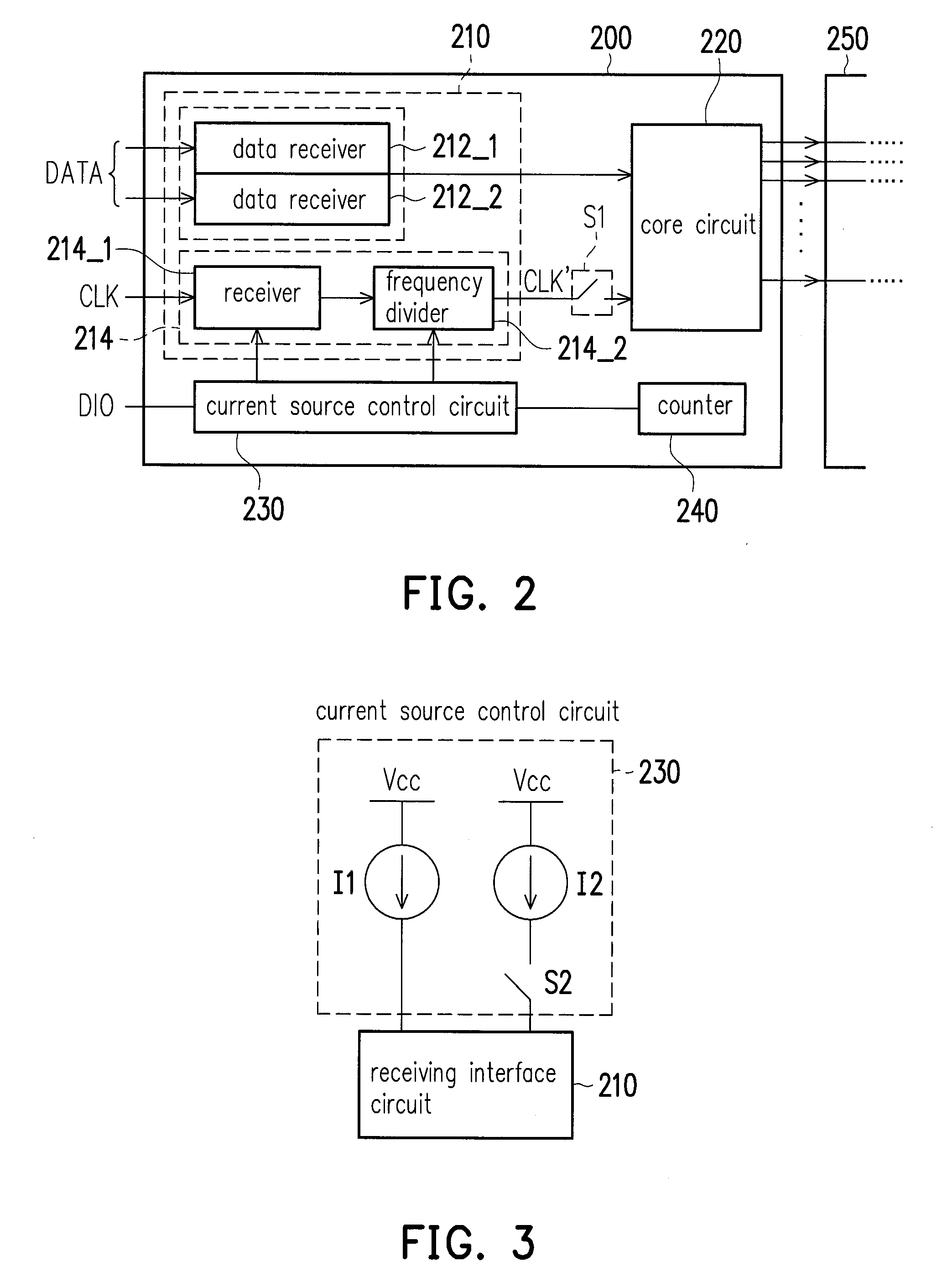
[0052]Next, the source driver 200 is reset in step S120. After the source driver 200 is reset, the current source control circuit 230 reduces the operating current of the receiving interface circuit 200 to the abnormal operating level (step S130) until the pixel data of the source driver 200 is appeared in the data signal DATA. For instance, in step S130 above, the current source control circuit 230 can reduce the operating current of the receiving interface circuit 210 in the source driver 200 to the abnormal operating level.

[0053]The current source control circuit 230 can d...

second embodiment

[0055]FIG. 6 is a flow chart illustrating an operation method of the source driver 200 depicted in FIG. 2 of the invention. Therein, steps S210 and S220 depicted in FIG. 6 can refer related description of steps S110 and S120 depicted in FIG. 5, so it is omitted hereinafter.

[0056]Referring to FIG. 2 and FIG. 6 together, the front-stage circuit (e.g., the timing controller) provides the clock signal CLK and the data signal DATA to the source driver 200 in step S210. The data receivers 212_1 and 212_2 and the clock receiver 214 in the receiving interface circuit 210 of the source driver 200 receive the data signal DATA and the clock signal CLK, respectively. After the source driver 200 is reset (step S220), the current source control circuit 230 reduces the operating current of the clock receiver 214 in the receiving interface circuit 210 to the abnormal operating level and suspends power supply to the data receiver 212_1 and 212_2 in the receiving interface circuit 210 (step S230). F...

third embodiment

[0058]FIG. 7 is a flow chart illustrating an operation method of the source driver depicted in FIG. 2 of the invention. Therein, steps S310, S320 and S340 depicted in FIG. 7 can refer related description of steps S110, S120 and S140 depicted in FIG. 5, so it is omitted hereinafter. Referring to FIG. 2 and FIG. 7 together, the front-stage circuit provides the clock signal CLK and the data signal DATA to the source driver 200 in step S310. Therein, the clock receiver 214 of the source driver 200 receives the clock signal CLK, and provides an internal clock CLK′ corresponding to the clock signal CLK to the core circuit 220 of the source driver 200 through the clock transmission path. After the source driver 200 is reset (step S320), the current source control circuit 230 reduces the operating current of the clock receiver 200 to the abnormal operating level, and the switch S1 turns off the clock transmission path to stop providing the internal clock CLK′ to the core circuit 220 (step ...


PUM


Abstract

A source driver and an operation method thereof are provided. The operation method includes following steps. A data signal is provided to the source driver. The operating current of the source driver is reduced to an abnormal operating level in period from the source driver is reset to before a pixel data of the source driver is appeared in the data signal. The operation current of the source driver is restored to a normal operating level when the pixel data of the source driver is appeared in the data signal.

Description

CROSS-REFERENCE TO RELATED APPLICATION[0001]This application claims the priority benefit of Taiwan application serial no. 102128850, filed on Aug. 12, 2013. The entirety of the above-mentioned patent application is hereby incorporated by reference herein and made a part of this specification.BACKGROUND OF THE INVENTION[0002]1. Field of the Invention[0003]The invention relates to an operation method of an electronic device, and more particularly to a source driver and an operation method thereof.[0004]2. Description of Related Art[0005]Generally, when a conventional source driver (SD) transmits a data signal, in order to synchronize the data signal to be received, each source driver continues to receive a clock signal provided by a system, and generates a clock signal for synchronizing with each other, so as to avoid the source driver from missing or mistakenly taking data.[0006]FIG. 1 is a schematic diagram of operations in a conventional source driver. As shown in FIG. 1, it is sup...

Claims


Application Information

Patent Timeline
Patent Type & Authority Applications(United States)
IPC IPC(8): G09G5/00
CPCG09G5/008G09G3/20G09G2310/027G09G2310/08G09G2330/021G09G2370/08
Inventor LIN, LI-TANGLIN, CHIA-HUNGWANG, PEI-YE
Owner NOVATEK MICROELECTRONICS CORP
Why Eureka
Try Eureka