Electronic equipment and plug-and-play device thereof

Inactive Publication Date: 2015-02-12
WISTRON NEWEB
View PDF13 Cites 4 Cited by
  • Summary
  • Abstract
  • Description
  • Claims
  • Application Information

AI Technical Summary

Benefits of technology

[0008]In the invention, the applicant discovered that the high-frequency transmission of the universal serial bus 3.0 causes the transmission pins to generate a high-frequency electromagnetic wave, which is the reason why universal serial bus 3.0 generates noise. Therefore, shielding the transmission pins with the electromagnetic shielding frame can reduce the noise genera

Problems solved by technology

However, the universal serial bus 3.0 generates noise in wireless signal transmissions, particularly with high-frequency wireless signal transmissions.
The noise generated by the universal serial bus 3.0 may cause wireless transmission failure in a portable electronic device (for example, a noteb

Method used


Image

  • Electronic equipment and plug-and-play device thereof
  • Electronic equipment and plug-and-play device thereof
  • Electronic equipment and plug-and-play device thereof

Examples


Example

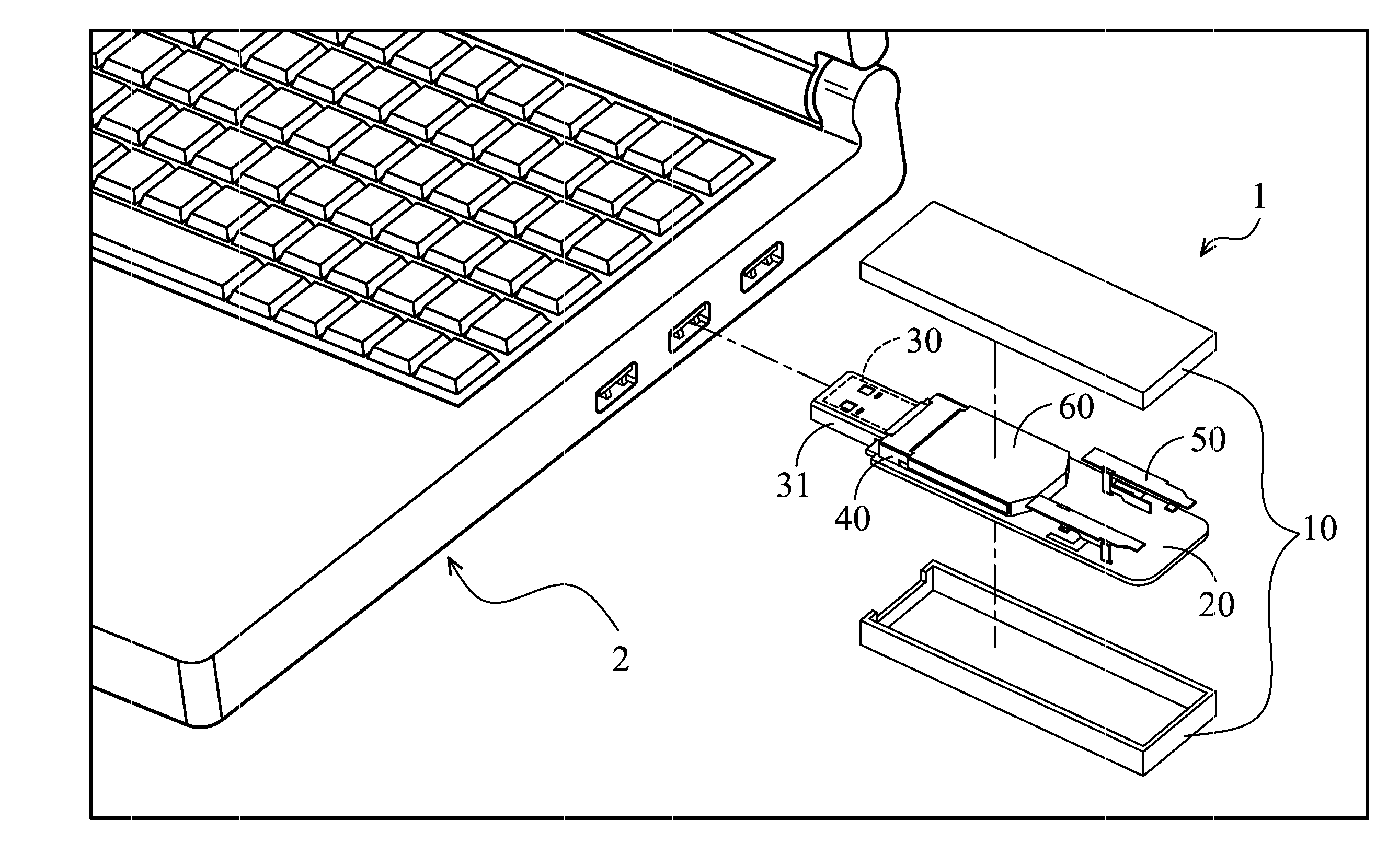
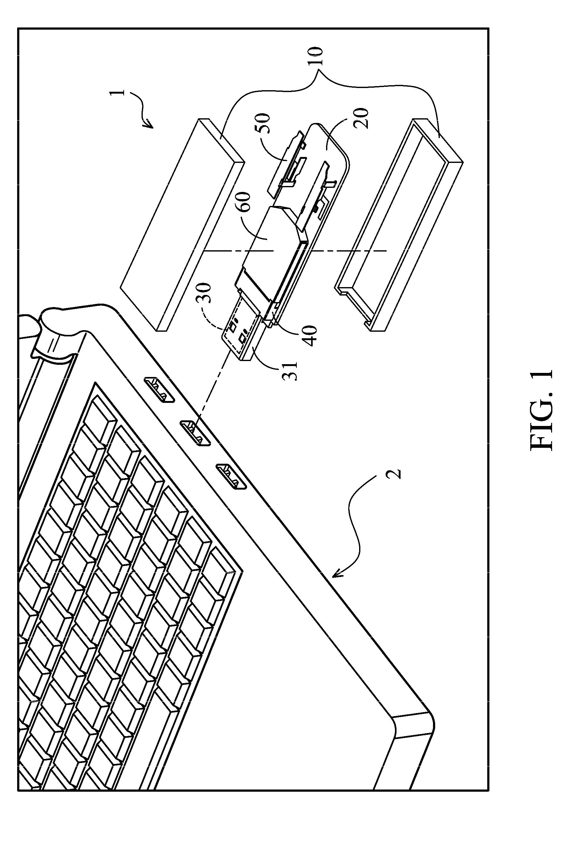
[0018]FIG. 1 shows a plug-and-play device 1 of a first embodiment of the invention, which comprises a device housing 10, a circuit board 20, a joint 30, an electromagnetic shielding frame 40, a wireless transmission module 50 and an electromagnetic shielding cover 60.

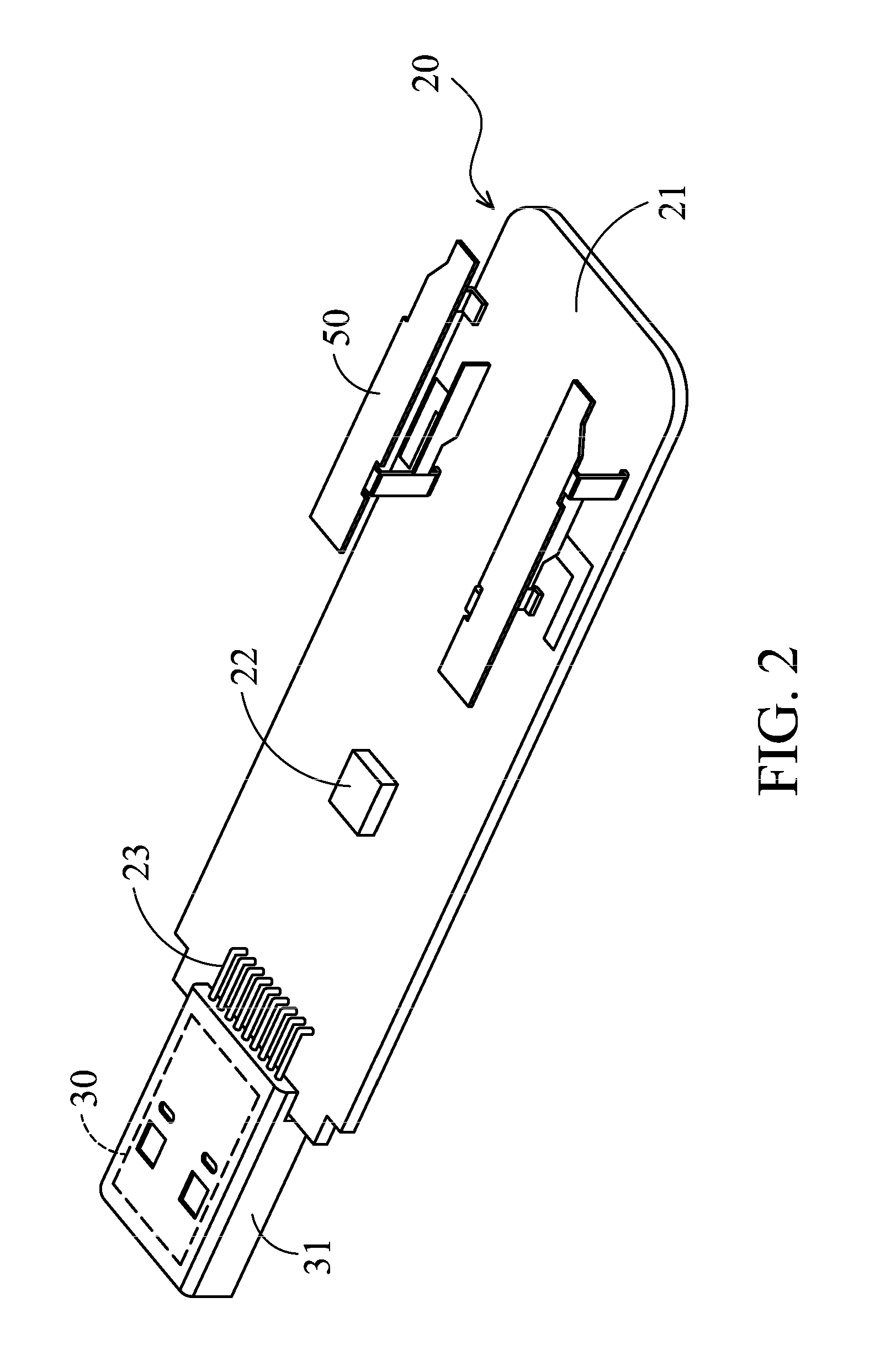
[0019]FIG. 2 shows the detailed structure of the circuit board 20 of the first embodiment of the invention. With reference to FIG. 2, the circuit board 20 is disposed in the device housing 10, including a substrate 21, a chip 22 and a plurality of transmission pins 23. The chip 22 and the transmission pins 23 are formed on the substrate 21. The transmission pins 23 are connected to the joint 30. With reference to FIGS. 1 and 2, the electromagnetic shielding frame 40 covers the transmission pins 23. The electromagnetic shielding cover 60 is connected to the electromagnetic shielding frame 40, and the electromagnetic shielding cover 60 covers the chip 22. The wireless transmission module 50 is disposed on the circuit boar...

Example

[0023]FIG. 4 shows a portion of a plug-and-play device 1′ of a second embodiment of the invention, wherein the electromagnetic shielding cover 60′ comprises a first bending portion 63 and a second bending portion 64. The first bending portion 63 is opposite to the second bending portion 64. The first bending portion 63 and the second bending portion 64 pass through the slot 91, and the first bending portion 63 and the second bending portion 64 abut the joint frame 31. The first bending portion 63 and the second bending portion 64 respectively abut a first lateral surface 33 and a second lateral surface 34 of the joint frame 31, and the first lateral surface 33 is opposite to the second lateral surface 34.

Example

[0024]FIG. 5 shows a portion of a plug-and-play device 1″ of a third embodiment of the invention, wherein the electromagnetic shielding cover 60″ comprises a first bending portion 65 and a second bending portion 66. The first bending portion 65 is opposite to the second bending portion 66. The first bending portion 65 and the second bending portion 66 extend over an outer surface of the electromagnetic shielding frame 40 to abut the joint frame 31. The first bending portion 65 and the second bending portion 66 respectively abut a first lateral surface 33 and a second lateral surface 34 of the joint frame 31.

[0025]Use of ordinal terms such as “first”, “second”, “third”, etc., in the claims to modify a claim element does not by itself connote any priority, precedence, or order of one claim element over another or the temporal order in which acts of a method are performed, but are used merely as labels to distinguish one claim element having a certain name from another element having t...


PUM


Abstract

A plug-and-play device is provided. The plug-and-play device includes a device housing, a circuit board, a joint and an electromagnetic shielding frame. The circuit board is disposed in the device housing, including a substrate and a plurality of transmission pins, wherein the transmission pins are formed on the substrate. The transmission pins are connected to the joint. The electromagnetic shielding frame covers the transmission pins.

Description

CROSS REFERENCE TO RELATED APPLICATIONS[0001]This Application claims priority of Taiwan Patent Application No. 102214968, filed on Aug. 9, 2013, the entirety of which is incorporated by reference herein.BACKGROUND OF THE INVENTION[0002]1. Field of the Invention[0003]The present invention relates to a plug-and-play device, and in particular to a plug-and-play device utilized to transmit a wireless signal.[0004]2. Description of the Related Art[0005]The universal serial bus with specification higher than 3.0 is popular, as it transmits data at high speeds. However, the universal serial bus 3.0 generates noise in wireless signal transmissions, particularly with high-frequency wireless signal transmissions. The noise generated by the universal serial bus 3.0 may cause wireless transmission failure in a portable electronic device (for example, a notebook). If a plug-and-play wireless transmission device utilizes universal serial bus 3.0, failure will occur in wireless transmissions, part...

Claims


Application Information

Patent Timeline
IPC IPC(8): H05K9/00H05K7/14
CPCH05K7/1452H05K9/0009H05K5/0278H05K9/0018H05K9/0032
Inventor PENG, CHIEN-MINGLIN, CHI-TE
Owner WISTRON NEWEB
Why Eureka
Try Eureka