Power circuit of displaying device

a power circuit and display device technology, applied in the field of power circuits, can solve the problems of control of the switch of the charge pump, excess power consumption, power consumption, etc., and achieve the effect of increasing the output voltage of the power circuit, sufficient rise rate, and improving the switching frequency or capacitance of the charge pump

Active Publication Date: 2015-02-19
SITRONIX TECH CORP
View PDF11 Cites 2 Cited by
  • Summary
  • Abstract
  • Description
  • Claims
  • Application Information

AI Technical Summary

Benefits of technology

[0012]Thereby, by improving the switching frequency or capacitance of the charge pump in a voltage conversion time of the plurality of scan driving signals, the rise rate of the output voltage of the power circuit is enhanced for facilitating the scan driver to provide a voltage having sufficient rise rate in the voltage conversion time of the scan driving signal. Besides, in the voltage holding time of the scan driving signal, the switching frequency or capacitance of the charge pump in the power circuit can be reduced for reducing the rise rate of the output voltage provided by the power circuit. Consequently, the effect of reducing power consumption can be achieved.
[0013]Moreover, the power circuit of display device according to the present invention further comprises a level detecting unit, which detects the output voltage of a charge pump and outputs a detecting signal to the control circuit according to the output voltage. The control circuit further outputs the clock signal or the capacitance adjusting signal to the charge pump according to the detecting signal for controlling the switching frequency or capacitance of the charge pump. Thereby, the present invention uses the level detecting unit to detect the output voltage of the charge pump for controlling the switching frequency or capacitance of the charge pump. Hence, the objective of saving power can be achieved.

Problems solved by technology

Nonetheless, there are many drawbacks to control the switches of the charge pump using the fixed-frequency clock.
Nonetheless, the power consumption increases as well.
Nonetheless, higher multiple and switching frequency reduce the voltage boosting efficiency and the voltage conversion efficiency, resulting in excess power consumption.
The high multiple and switching frequency in the voltage holding time result in excess power consumption.

Method used


Image

  • Power circuit of displaying device
  • Power circuit of displaying device
  • Power circuit of displaying device

Examples


first embodiment

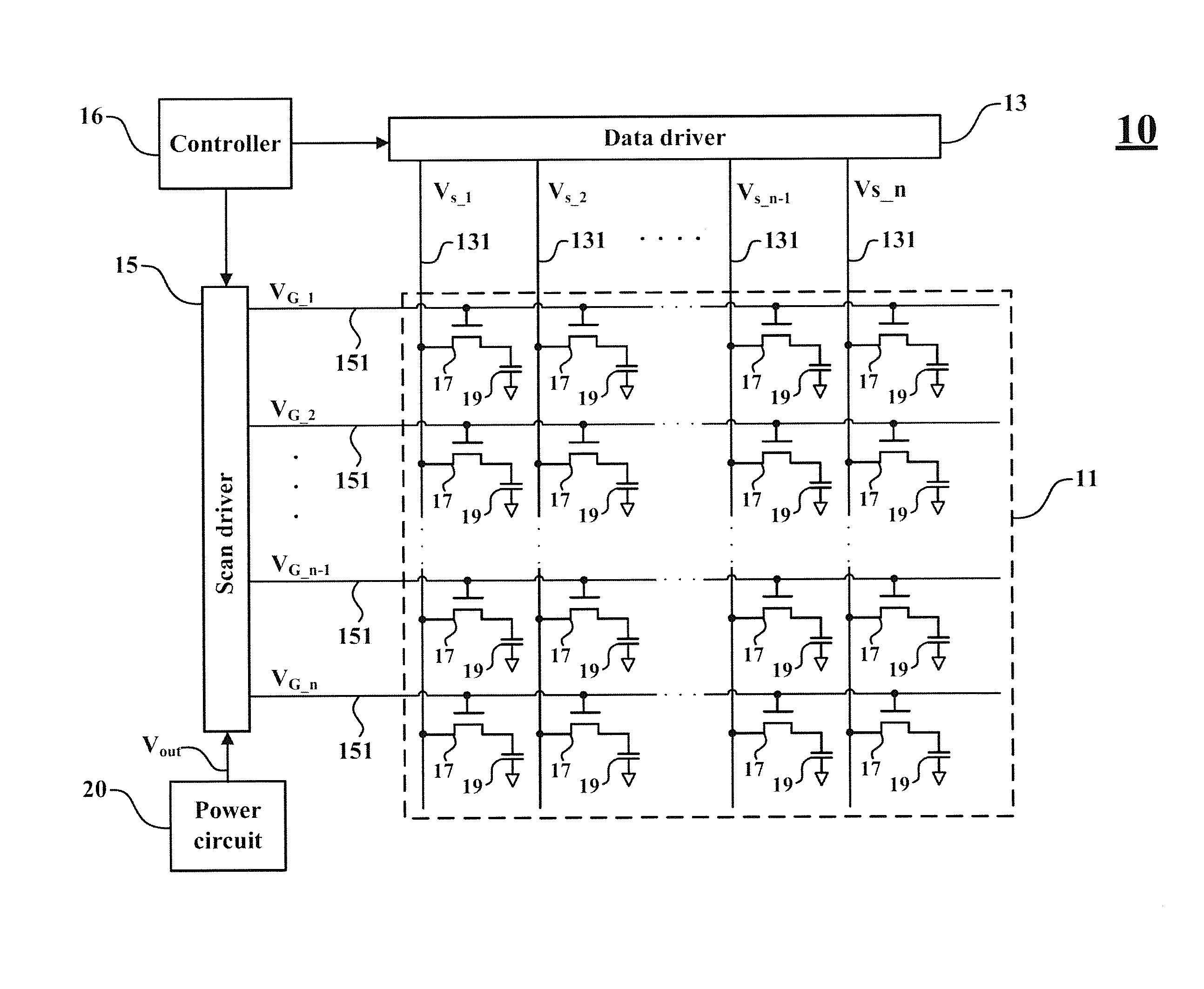
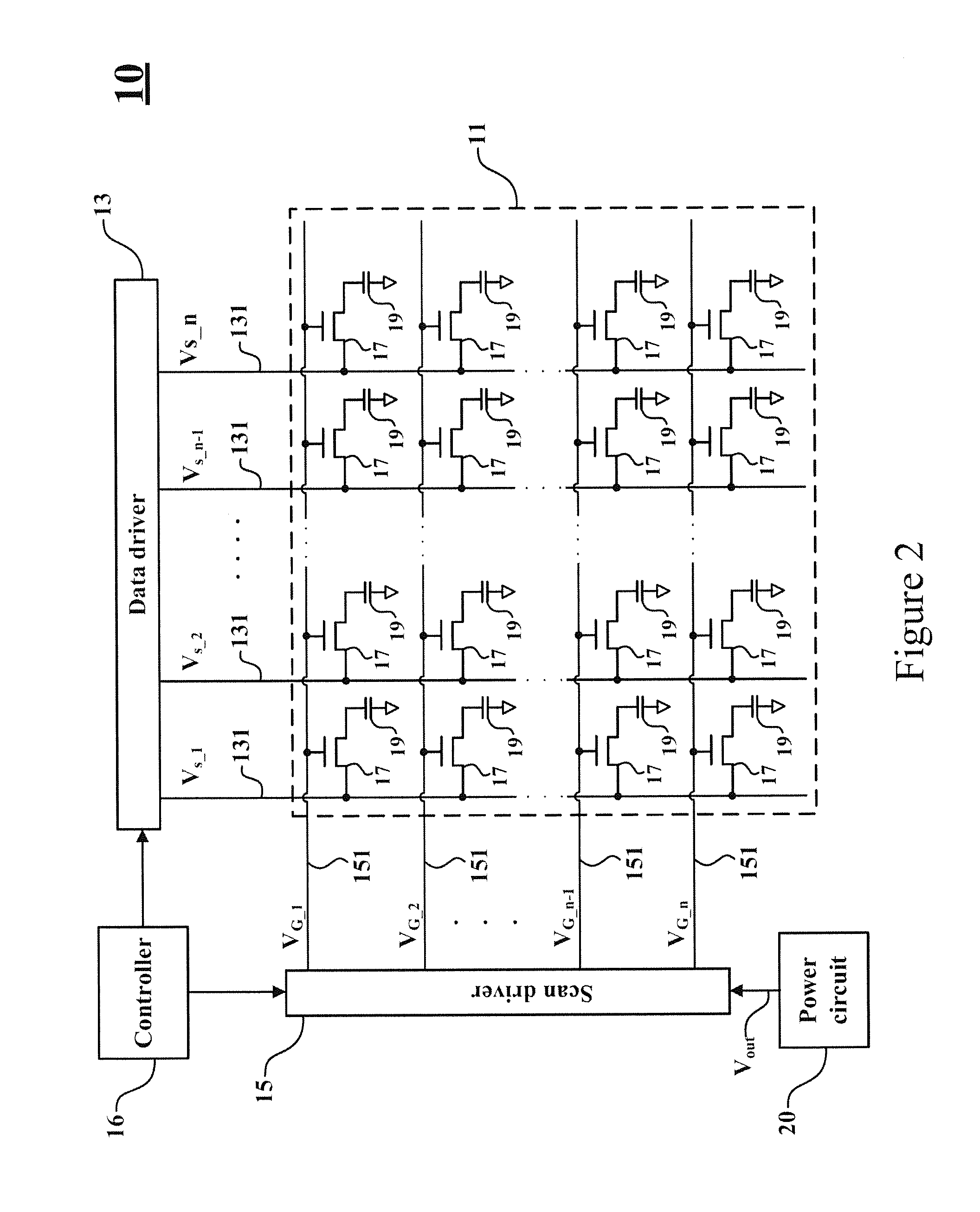
[0028]Please refer to FIG. 2, which shows a circuit diagram of the displaying device according to the power circuit of displaying device according to the present invention. As shown in the figure, the power circuit according to the present invention can be applied to various displaying devices such as thin-film transistor (TFT), twisted nematic (TN), and super twisted nematic (STN) displaying devices. The displaying device 10 comprises a panel 11, a data driver 13, a scan driver 15, a controller 16, and a power circuit 20. According to the present embodiment, the power circuit 20 of the displaying device 10 according to the present invention is applied, but not limited, to a TFT displaying device 10. The panel 11 according to the present embodiment has a plurality of TFTs 17 and a plurality of liquid crystal capacitors 19. The plurality of liquid crystal capacitors 19 are coupled to the plurality of TFTs, respectively. The gates of the plurality of TFTs 17 are coupled to the scan dr...

third embodiment

[0053]Please refer to FIG. 10, which shows a waveform of the output voltage according to the present invention. As shown in the figure, when the output voltage Vout is raised to the first threshold value, the frequency adjusting unit 2031 and / or the capacitance adjusting unit 2033 lower the switching frequency and / or the capacitance of the charging capacitors of the charge pump 205 according to the voltage detecting signal Vtemp for lowering the rise rate of the output voltage Vout1. When the output voltage Vout1 is raised to the second threshold value, the switching frequency and / or the capacitance of the charging capacitors of the charge pump 205 are reduced again for further lowering the rise rate of the output voltage Vout1.

[0054]Please refer to FIG. 11, which shows a circuit block diagram of the power circuit of displaying device according to the fourth embodiment of the present invention. As shown in the figure, the difference between the present embodiment and the second embo...


PUM


Abstract

The present invention relates to a power circuit of displaying device, which comprises a timing controller, a control circuit, and a charge pump (single or multiple stages). The timing controller outputs a timing control signal to the control circuit. The control circuit outputs a clock signal or a capacitance adjusting signal according to the timing control signal. The charge pump receives the input voltage and outputs an output voltage according to the clock signal or the capacitance adjusting signal. The output voltage is provided to the scan driver for generating a plurality of scan driving signals. Accordingly, by increasing the rise rate of the output voltage of the charge pump in the voltage conversion time and reducing the rise rate of the output voltage close to the voltage holding time, the present invention can achieve the effect of reducing the power consumption.

Description

FIELD OF THE INVENTION[0001]The present invention relates to a power circuit, and particularly to a power circuit of display device.BACKGROUND OF THE INVENTION[0002]Many current commercial electronic devices usually require different voltage levels as power sources. Thereby, charge pumps are disposed for using existing voltages to generate different voltage levels. The charge pump circuit according to the prior art generally comprises a voltage source, at least a charging capacitor, an output capacitor, a plurality of switches, and a fixed-frequency clock for controlling multiple switches to generate different voltage levels. First, the voltage source and the charging capacitor are connected in parallel using the plurality of switches for charging the charging capacitor to a voltage level. Then, the charging capacitor is connected in series with the output capacitor. After repeated for a plurality of cycles, the voltage across the output capacitor will be raised to a voltage level m...

Claims


Application Information

Patent Timeline
Patent Type & Authority Applications(United States)
IPC IPC(8): G09G3/36
CPCG09G3/3696G09G2330/02G09G3/3611G09G3/3648H02M1/36H02M3/07H02M1/0006
Inventor WU, KAI-YILIAO, KUAN-CHAOLU, HUNG-YU
Owner SITRONIX TECH CORP
Why Eureka
Try Eureka