Liquid crystal display device

a liquid crystal display and display device technology, applied in non-linear optics, instruments, optics, etc., can solve problems such as problems such as viewing angle properties, and achieve the effects of preventing the occurrence of domains, excellent contrast, and high definition

Active Publication Date: 2015-02-26
JAPAN DISPLAY INC
View PDF3 Cites 9 Cited by
  • Summary
  • Abstract
  • Description
  • Claims
  • Application Information

AI Technical Summary

Benefits of technology

[0016]An object of the present invention is to achieve a structure for preventing the occurrence of the domain in an IPS mode liquid crystal display device with a high definition screen.
[0022]According to the present invention, it is possible to prevent the occurrence of a domain in a liquid crystal display device with small pixels, or high definition. As a result, it is possible to provide a liquid crystal display device with excellent contrast.

Problems solved by technology

The viewing angle property is a problem for the liquid crystal display device.

Method used


Image

  • Liquid crystal display device
  • Liquid crystal display device
  • Liquid crystal display device

Examples


first embodiment

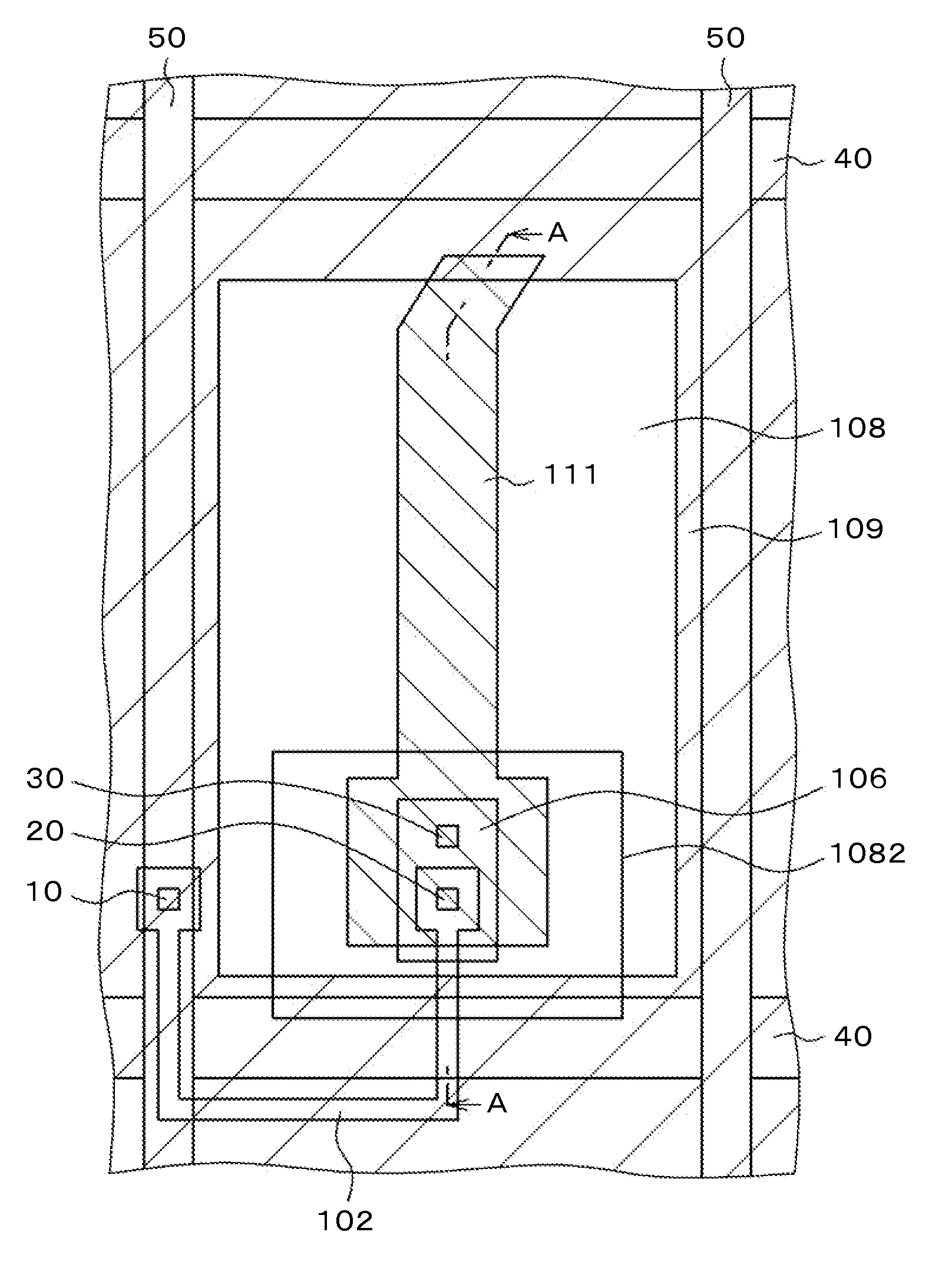
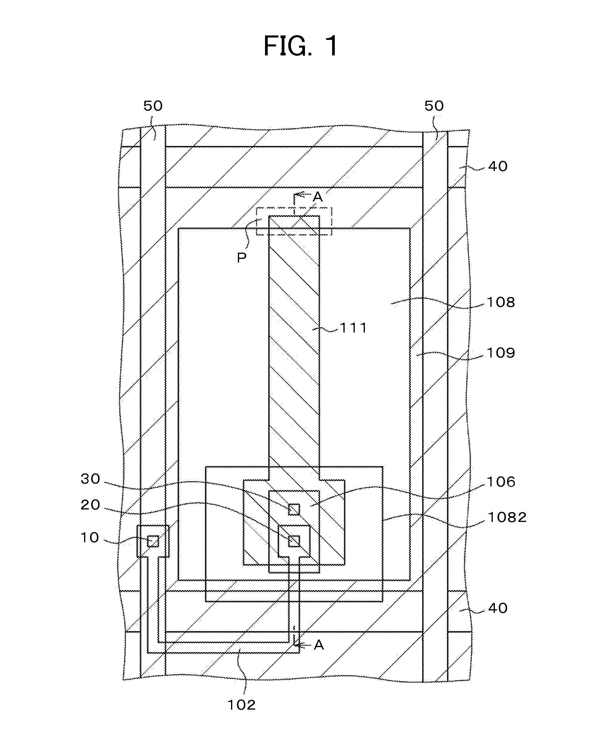
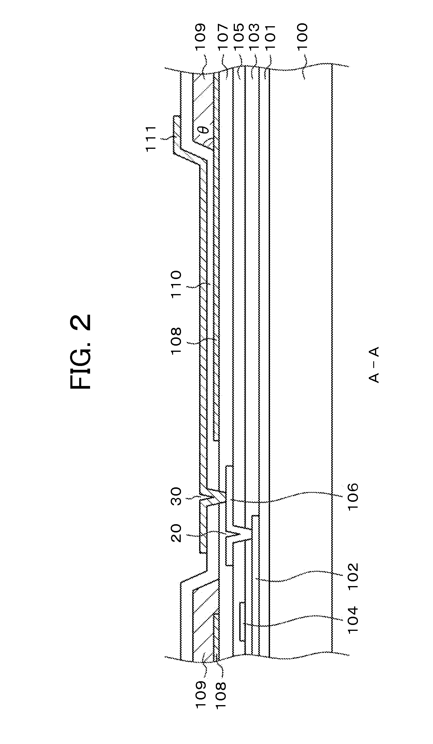
[0041]FIG. 1 is a plan view of a pixel structure according to a first embodiment. FIG. 2 is a cross-sectional view taken along line A-A of FIG. 1. FIG. 1 is the same as FIG. 11 in which the semiconductor layer 102 is formed of poly-Si between the video signal lines 50 and the source electrode 106, a first TFT is formed using the scanning line 40 as a gate electrode on the left side below the video signal line 50, and a second TFT is formed and connected to the first TFT in series. The region of the semiconductor layer 102 below the scanning line 40 is a channel portion, and the other region is doped with impurities to form a conductor. The video signal line 50 is connected to the first TFT through the first through hole 10. Then, the source electrode 106 is connected to the second TFT through the second through hole 20.

[0042]The pixel electrode 111 is connected to the source electrode 106 through the third through hole 30. In the present embodiment, the pixel electrode 111 has a lon...

second embodiment

[0051]FIG. 5 is a plan view of the pixel portion, which shows a second embodiment of the present invention. FIG. 6 is a cross-sectional view taken along line B-B of FIG. 5. The present embodiment is different from the first embodiment in that the first electrode formed flat on the lower layer is used as the pixel electrode 111, and that the second electrode on the upper layer with the second interlayer insulating film 110 therebetween is used as the counter electrode 108 with a slit 1081.

[0052]FIG. 5 is the same as the first embodiment in which the organic passivation film 109 is removed in the pixel surrounded by the scanning lines 40 and the video signal lines 50, except the periphery of the pixel. In FIG. 5, the pixel electrode 111 marked by diagonal lines is formed flat in the pixel. The peripheral portion of the counter electrode 108 rides over the organic passivation film 109 marked by diagonal lines, which is formed in the vicinity of the pixel. In FIG. 5, the source portion ...

third embodiment

[0058]FIG. 7 is a plan view of a third embodiment of the present invention. FIG. 8 is a cross-sectional view taken along line C-C of FIG. 7. The third embodiment is different from the second embodiment in that the inorganic passivation film 107 shown in FIG. 6 of the second embodiment is not present, and that the pixel electrode 111 and the source electrode 106 are formed on the same first interlayer insulating film 105. Thus, the third through hole is not present in FIGS. 7 and 8. The source electrode 106 and a portion of the pixel electrode 111 overlap to establish electrical conductivity. The other structures are the same as the second embodiment.

[0059]In other words, in FIG. 7, the organic passivation film 109 marked by diagonal lines is present in the vicinity of the rectangular pixel electrode 111 marked by diagonal lines. Then, the counter electrode 108 with the slit 1081 covers the entire electrode. FIG. 8 is a cross-sectional view taken along line C-C of FIG. 7. FIG. 8 is t...


PUM

PropertyMeasurementUnit
thicknessaaaaaaaaaa
inclination angleaaaaaaaaaa
insulatingaaaaaaaaaa

Abstract

In an IPS mode liquid crystal display device, a counter electrode is formed flat on a first insulating film. A second insulating film is formed in the peripheral portion of the counter electrode. A third insulating film is formed so as to cover the counter electrode and the second insulating film. A pixel electrode is formed on the third insulating film. The second and third insulating films are present between the pixel electrode and the counter electrode in the periphery of the pixel. The third insulating film is present between the pixel electrode and the counter electrode in the portion other than the peripheral portion of the pixel. An electric field between the pixel electrode and the counter electrode is smaller in the periphery of the pixel than in the vicinity of the center of the pixel, to prevent the occurrence of a domain in the periphery of the pixel.

Description

CLAIM OF PRIORITY[0001]The present application claims priority from Japanese Patent Application JP 2013-170268 filed on Aug. 20, 2013, the content of which is hereby incorporated by reference into this application.BACKGROUND[0002]The present invention relates to a display device, and more particularly, to a liquid crystal display device with a high definition screen in a lateral electric field mode that prevents the occurrence of a domain.[0003]A liquid crystal display device includes a TFT substrate in which pixels having pixel electrodes, thin film transistors (TFT) and the like are formed in a matrix, as well as a counter substrate in which color filters and the like are formed at the positions corresponding to the pixel electrodes of the TFT substrate. The counter substrate is disposed opposite the TFT substrate with a liquid crystal interposed between the TFT substrate and the counter substrate. Then, the transmittance of light caused by liquid crystal molecules is controlled a...

Claims


Application Information

Patent Timeline
Patent Type & Authority Applications(United States)
IPC IPC(8): G02F1/1343G02F1/1362G02F1/1337G02F1/1333
CPCG02F1/134363G02F1/133345G02F1/133707G02F1/136277G02F1/136227G02F1/134372
Inventor SAKAI, TAKESHIISHIGAKI, TOSHIMASATOMIOKA, YASUSHI
Owner JAPAN DISPLAY INC
Why Eureka
Try Eureka