

Device for depositing a layer on a semiconductor wafer by means of vapour deposition
a technology of vapour deposition and semiconductor wafer, which is applied in the direction of chemical vapor deposition coating, coating, metallic material coating process, etc., can solve the problem that the optimization of process parameters cannot avoid local temperature increase, and achieve the effect of increasing uniformizing the thickness of the layer
Active Publication Date: 2015-02-26
SILTRONIC AG
View PDF5 Cites 3 Cited by
- Summary
- Abstract
- Description
- Claims
- Application Information
AI Technical Summary
Benefits of technology
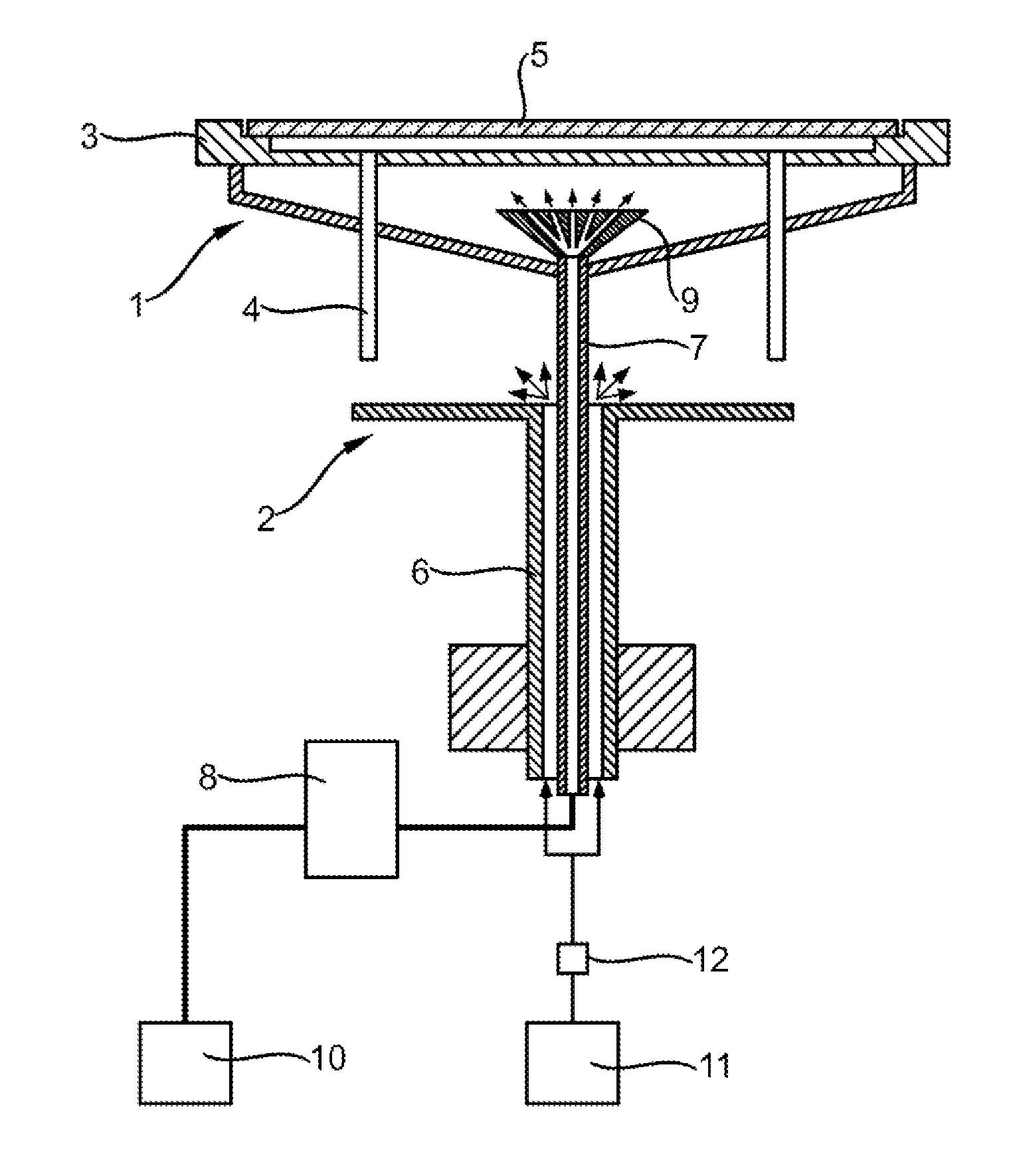
The patent text describes an apparatus and method for depositing layers on semiconductor wafers using vapor deposition. The invention aims to achieve a more uniform layer thickness by reducing a temperature increase in the center region of the susceptor, which is caused by a temperature increase in the center region of the susceptor during operation. The apparatus includes a susceptor, a shaft, a gas distributor head, and a line for feeding cooling gas. By cooling the rear side of the susceptor using the cooling gas, the method improves the uniformity of layer thickness on semiconductor wafers.
Problems solved by technology
It has now been surprisingly and unexpectedly discovered that the increased layer thickness found in the center of the coated semiconductor wafers is attributable to a temperature increase in the center region of the susceptor, and that this local temperature increase cannot be avoided by optimization of process parameters.
Method used
View moreImage
Smart ImageViewing Examples

Examples
example
[0027]As shown by the comparison of FIG. 3 and FIG. 4, the radial distribution of the later thickness h is significantly more uniform if the apparatus according to the invention is used.
Login to View More PUM
| Property | Measurement | Unit |
|---|---|---|
| diameter | aaaaa | aaaaa |
| diameter | aaaaa | aaaaa |
| length | aaaaa | aaaaa |
Abstract
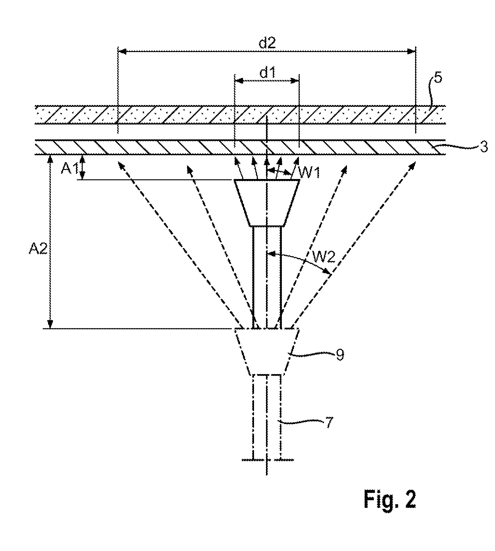
Uniformity of vapor deposited coatings on semiconductor wafers is improved by employing an apparatus having a gas distributor head below a susceptor onto which the wafer is placed, the gas distributor head directing a fan of cooling gas at the rear side of the susceptor. The ratio of the diameter of the cooled section of the susceptor to the diameter D of the wafer is preferably from 0.1 to 0.4.
Description
CROSS REFERENCE TO RELATED APPLICATIONS[0001]This application is the U.S. National Phase of PCT Appln. No. PCT / EP2013 / 056011 filed Mar. 22, 2013, which claims priority to German Application No. 10 2012 205 616.5 filed Apr. 4, 2012, the disclosures of which are incorporated in their entirety by reference herein.BACKGROUND OF THE INVENTION[0002]1. Field of the Invention[0003]The invention relates to an apparatus for depositing a layer on a semiconductor wafer by means of vapor deposition, and to a method that uses the apparatus.[0004]2. Description of the Related Art[0005]US2004 / 0144323 A1 discloses an apparatus for depositing a layer on a semiconductor wafer, comprising an upper and a lower cover composed of transparent material and a side wall, which together define a reactor chamber. The reactor chamber is divided by a susceptor into an upper reactor chamber and a lower reactor chamber. The susceptor supports a semiconductor wafer to be coated and itself rests on arms of a supporti...
Claims
Login to View More Application Information
Patent Timeline
 Patent Type & AuthorityApplications(United States)
IPC IPC(8): H01L21/687C23C16/455C23C16/46H01L21/02C23C16/458
CPCH01L21/68785H01L21/02532H01L21/0262C23C16/45502C23C16/4584C23C16/466C23C16/4586H01L21/02381H01L21/683H01L21/67253
InventorBRENNINGER, GEORG
OwnerSILTRONIC AG