Vertical tunnel field effect transistor

a technology of field effect transistor and tunnel tunnel, which is applied in the direction of diodes, semiconductor devices, electrical apparatus, etc., can solve the problem that the transistor may present scaling challenges

Active Publication Date: 2015-03-12
QUALCOMM INC
View PDF3 Cites 41 Cited by
  • Summary
  • Abstract
  • Description
  • Claims
  • Application Information

AI Technical Summary

Benefits of technology

[0004]A vertical tunnel field effect transistor (TFET) and a method of fabrication are disclosed. A fin-type vertical TFET may include a source region and a drain region that are vertically coupled via a channel region. A vertical tunnel may be formed within the channel region to create a conduction path between the source region and the drain region. The length of the vertical tunnel may be dependent on the height of the channel region. The fin-type vertical TFET may also include a gate with an adjustable width. For example, an amount of saturation current that flows through the vertical tunnel may be adjusted (e.g., increased or decreased) in response to changing the width of the gate.

Problems solved by technology

However, because tunnel CMOS transistors are typically planar, such tunnel CMOS transistors may present scaling challenges for sub-22 nanometer (nm) process dimensions and beyond.

Method used


Image

  • Vertical tunnel field effect transistor
  • Vertical tunnel field effect transistor
  • Vertical tunnel field effect transistor

Examples


Embodiment Construction

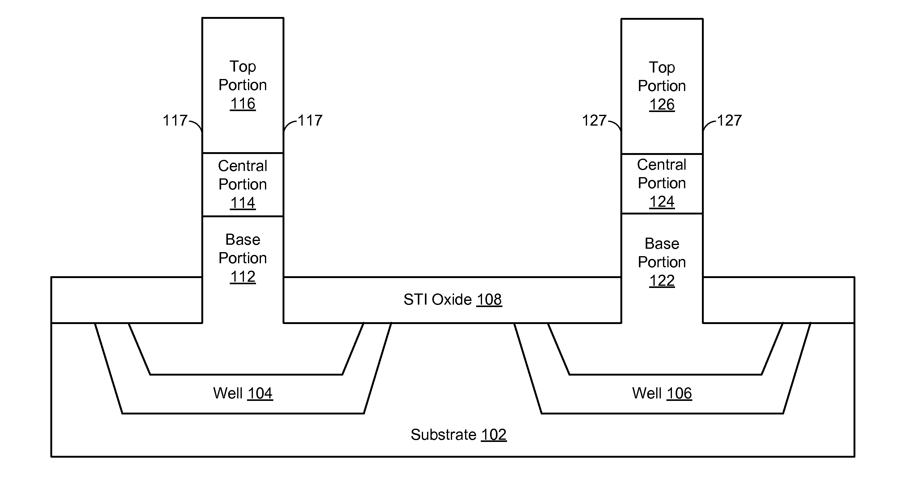
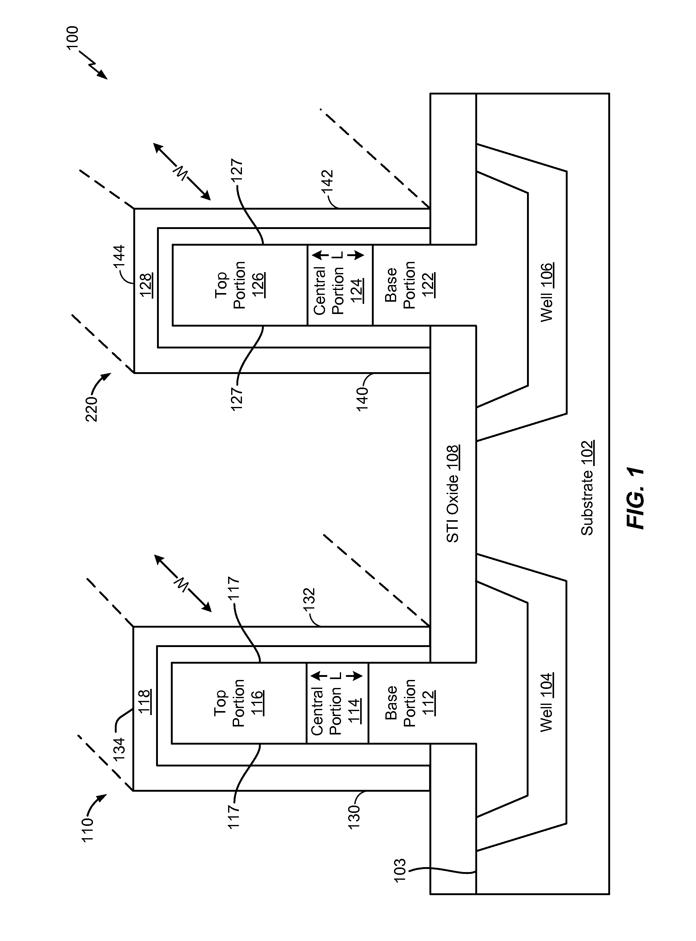
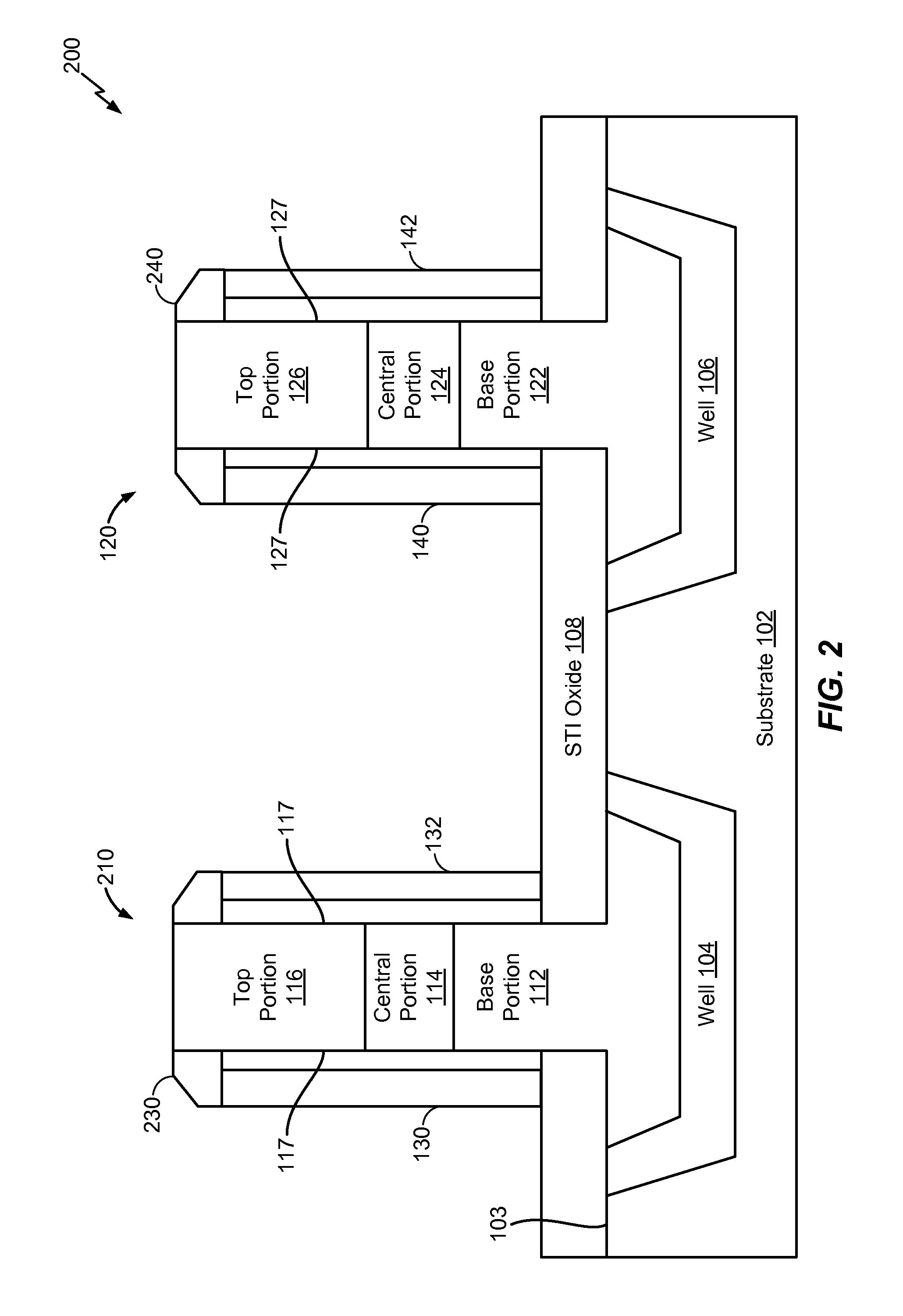
[0021]Particular embodiments of vertical tunnel field effect transistor devices and methods of fabrication are presented in this disclosure. It should be appreciated, however, that the concepts and insights applied to the particular embodiments with respect to designs of the vertical tunnel field effect transistor devices and with respect to how to make the vertical tunnel field effect transistor devices may be embodied in a variety of contexts. The particular embodiments presented are merely illustrative of specific ways to design and make the vertical tunnel field effect transistor devices and do not limit the scope of this disclosure.

[0022]The present disclosure describes the particular embodiments in specific contexts. However, features, methods, structures or characteristics described according to the particular embodiments may also be combined in suitable manners to form one or more other embodiments. In addition, figures are used to illustrate the relative relationships betwe...


PUM

PropertyMeasurementUnit
dielectric constantaaaaaaaaaa
lengthaaaaaaaaaa

Abstract

A tunnel field transistor (TFET) device includes a fin structure that protrudes from a substrate surface. The fin structure includes a base portion proximate to the substrate surface, a top portion, and a first pair of sidewalls extending from the base portion to the top portion. The first pair of sidewalls has a length corresponding to a length of the fin structure. The fin structure also includes a first doped region having a first dopant concentration at the base portion of the fin structure. The fin structure also includes a second doped region having a second dopant concentration at the top portion of the fin structure. The TFET device further includes a gate including a first conductive structure neighboring a first sidewall of the first pair of sidewalls. A dielectric layer electrically isolates the first conductive structure from the first sidewall.

Description

I. FIELD[0001]The present disclosure is generally related to a vertical tunnel field effect transistor.II. DESCRIPTION OF RELATED ART[0002]Advances in technology have resulted in smaller and more powerful computing devices. For example, there currently exist a variety of portable personal computing devices, including wireless computing devices, such as portable wireless telephones, personal digital assistants (PDAs), and paging devices that are small, lightweight, and easily carried by users. More specifically, portable wireless telephones, such as cellular telephones and internet protocol (IP) telephones, may communicate voice and data packets over wireless networks. Further, many such wireless telephones include other types of devices that are incorporated therein. For example, a wireless telephone may also include a digital still camera, a digital video camera, a digital recorder, and an audio file player. Also, such wireless telephones may process executable instructions, includ...

Claims


Application Information

Patent Timeline
Patent Type & Authority Applications(United States)
IPC IPC(8): H01L29/66H01L29/78
CPCH01L29/66977H01L29/7827H01L29/66795H01L29/66356H01L29/7391
Inventor LI, XIACAI, MINGYANG, BIN
Owner QUALCOMM INC
Why Eureka
Try Eureka