Semiconductor device and fabrication method thereof and semiconductor structure

a semiconductor and semiconductor technology, applied in semiconductor devices, semiconductor/solid-state device details, electrical devices, etc., can solve the problems of solder bridging and easy bridging between solder bumps, and achieve the effect of reducing the fabrication cost of the semiconductor device and the semiconductor structure, increasing the contact area, and increasing the width

Active Publication Date: 2015-03-12
SILICONWARE PRECISION IND CO LTD
View PDF8 Cites 9 Cited by
  • Summary
  • Abstract
  • Description
  • Claims
  • Application Information

AI Technical Summary

Benefits of technology

[0027]By dispensing with the insulating layer as required in the prior art, the present invention reduces the fabrication cost of the semiconductor device and the semiconductor structure. Further, the first conductive portions can be greater in width than conventional copper pillars so as to increase the contact area between the first conductive portions and the UBM layer, thereby reducing stresses therebetween. Furthermore, the second conductive portions can be less in width than the conventional copper pillars so as to increase the distance between adjacent second conductive portions, thus preventing solder bridging from occurring therebetween and increasing the produce yield.

Problems solved by technology

However, as I / O counts increase and the distance between the solder bumps decreases, solder bridging easily occurs between the solder bumps.
But as the distance between the copper pillar bumps continuously decreases, solder bridging can still occur.

Method used


Image

  • Semiconductor device and fabrication method thereof and semiconductor structure
  • Semiconductor device and fabrication method thereof and semiconductor structure
  • Semiconductor device and fabrication method thereof and semiconductor structure

Examples


Embodiment Construction

[0031]The following illustrative embodiments are provided to illustrate the disclosure of the present invention, these and other advantages and effects can be apparent to those in the art after reading this specification.

[0032]It should be noted that all the drawings are not intended to limit the present invention. Various modifications and variations can be made without departing from the spirit of the present invention. Further, terms such as “first”, “second”, “on”, “a” etc. are merely for illustrative purposes and should not be construed to limit the scope of the present invention.

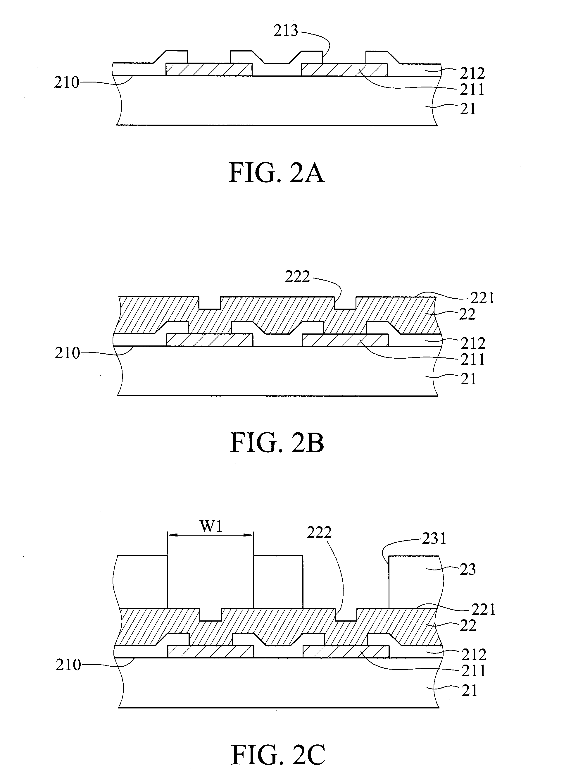
[0033]FIGS. 2A to 2N are schematic cross-sectional views showing a semiconductor device and a fabrication method thereof according to a first embodiment of the present invention.

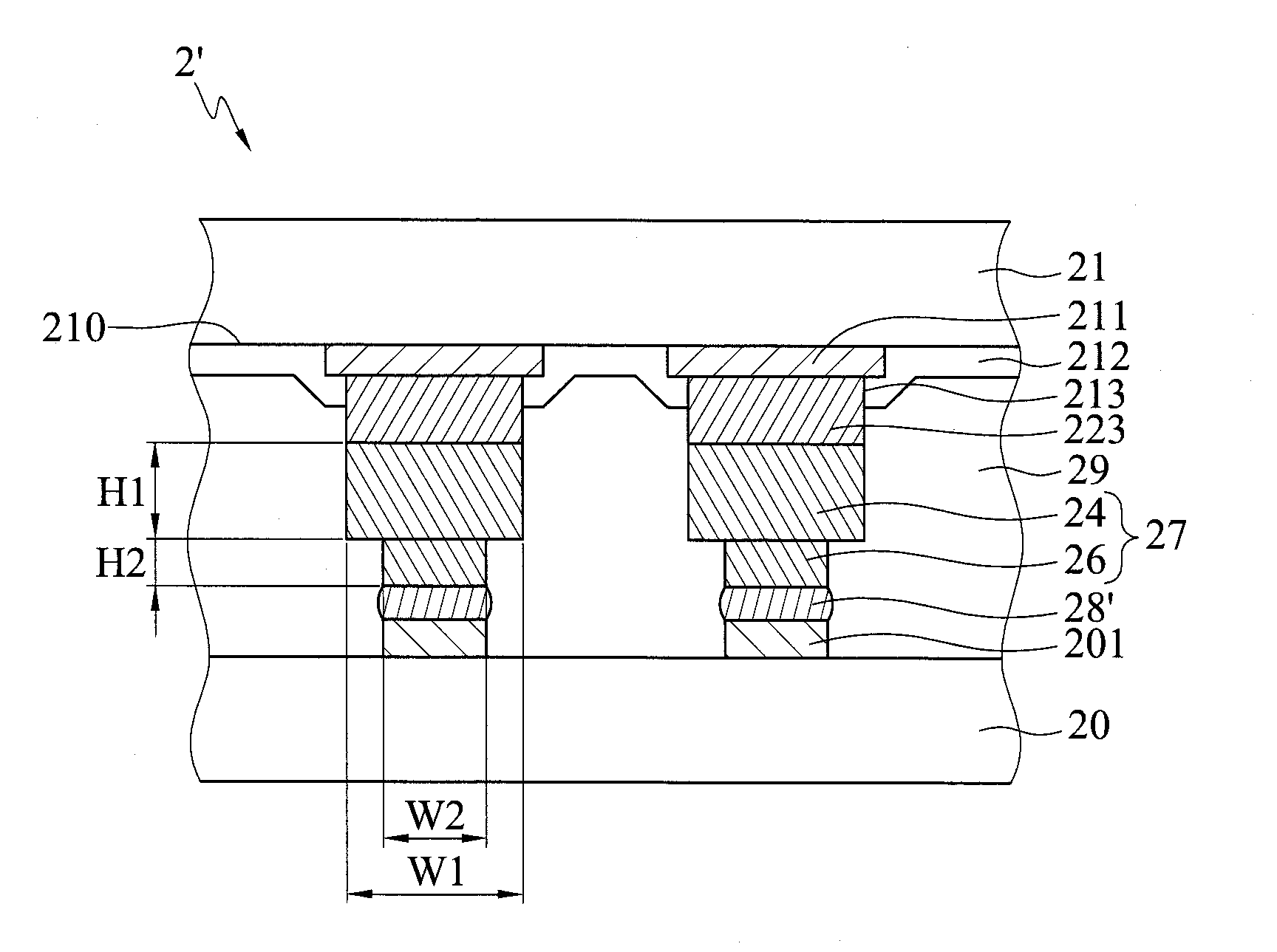
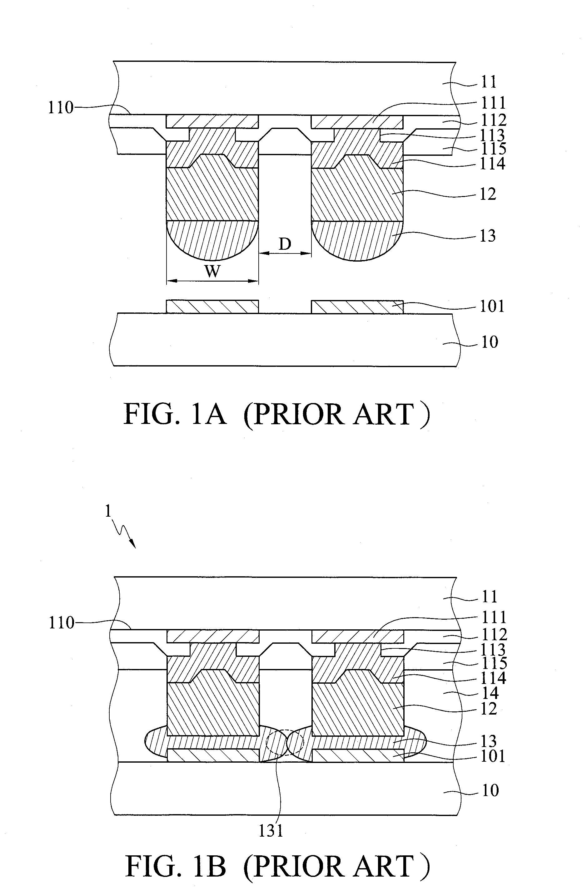
[0034]Referring to FIG. 2A, a semiconductor component 21 such as a semiconductor chip is provided. The semiconductor component 21 has at least two adjacent bonding pads 211 formed on a surface 210 thereof. Further, a passivatio...


PUM


Abstract

A semiconductor device is disclosed, which includes: a substrate having a plurality of connecting pads; a semiconductor component having a plurality of bonding pads formed on a surface thereof and corresponding to the connecting pads and a UBM layer formed on the bonding pads; a plurality of conductive elements each having a first conductive portion and a second conductive portion sequentially formed on the UBM layer, wherein the second conductive portion is less in width than the first conductive portion; and a plurality of solder balls formed between the second conductive portions and the connecting pads for connecting the semiconductor component and the substrate, thereby preventing solder bridging from occurring between the adjacent conductive elements and reducing stresses between the conductive elements and the UBM layer.

Description

BACKGROUND OF THE INVENTION[0001]1. Field of the Invention[0002]The present invention relates to semiconductor devices and fabrication methods thereof and semiconductor structures, and more particularly, to a semiconductor device and a fabrication method thereof and a semiconductor structure for improving the product yield.[0003]2. Description of Related Art[0004]In a conventional flip-chip package, a plurality of solder bumps are formed on bonding pads of a chip for mounting the chip on a substrate. However, as I / O counts increase and the distance between the solder bumps decreases, solder bridging easily occurs between the solder bumps. To alleviate the problem, copper pillar bumps can be formed instead of the solder bumps. But as the distance between the copper pillar bumps continuously decreases, solder bridging can still occur.[0005]FIGS. 1A and 1B are schematic cross-sectional views showing a semiconductor device and a fabrication method thereof according to the prior art.[000...

Claims


Application Information

Patent Timeline
Patent Type & Authority Applications(United States)
IPC IPC(8): H01L23/00H01L21/768H01L23/498
CPCH01L24/14H01L21/76895H01L24/11H01L23/49816H01L2224/13005H01L23/3171H01L21/563H01L24/03H01L24/05H01L24/13H01L24/16H01L24/81H01L2224/034H01L2224/05558H01L2224/11462H01L2224/1147H01L2224/11849H01L2224/11903H01L2224/13017H01L2224/13083H01L2224/13147H01L2224/16057H01L2224/16238H01L2224/73204H01L2224/81191H01L2224/03912H01L2224/05572H01L2224/0401H01L2224/05009H01L2224/05022H01L2224/1134H01L2224/131H01L2924/3841H01L2224/16058H01L2224/1308H01L2924/00014H01L2924/00012H01L2924/206H01L2924/207H01L2924/014
Inventor LIN, CHANG-FUYAO, CHIN-TSAICHANG, HUNG-MINGCHUANG, MING-CHINHUANG, FU-TANG
Owner SILICONWARE PRECISION IND CO LTD
Why Eureka
Try Eureka