Method of fabricating a Si3N4/polycide structure using a dielectric sacrificial layer as a mask

a polycide structure and dielectric sacrificial layer technology, applied in the direction of semiconductor/solid-state device manufacturing, basic electric elements, electric apparatus, etc., can solve the problems of very detrimental si3n4 line bottoms to an accurate c1 dimension control

Inactive Publication Date: 2002-01-29
IBM CORP
View PDF5 Cites 55 Cited by
  • Summary
  • Abstract
  • Description
  • Claims
  • Application Information

AI Technical Summary

Benefits of technology

It is therefore a primary object of the present invention to provide an improved method of fabricating a composite Si3N4/

Problems solved by technology

However, because the BPSG layer surface is not perfectly planar, a chemical-mechanical polishing (CMP) step is required to get a mirror-like surface and reduce the BPSG layer thickness to 1400 nm.
As a consequence, polymer residuals are produced at the bottom of the BARL lines wh

Method used


Image

  • Method of fabricating a Si3N4/polycide structure using a dielectric sacrificial layer as a mask
  • Method of fabricating a Si3N4/polycide structure using a dielectric sacrificial layer as a mask
  • Method of fabricating a Si3N4/polycide structure using a dielectric sacrificial layer as a mask

Examples


Embodiment Construction

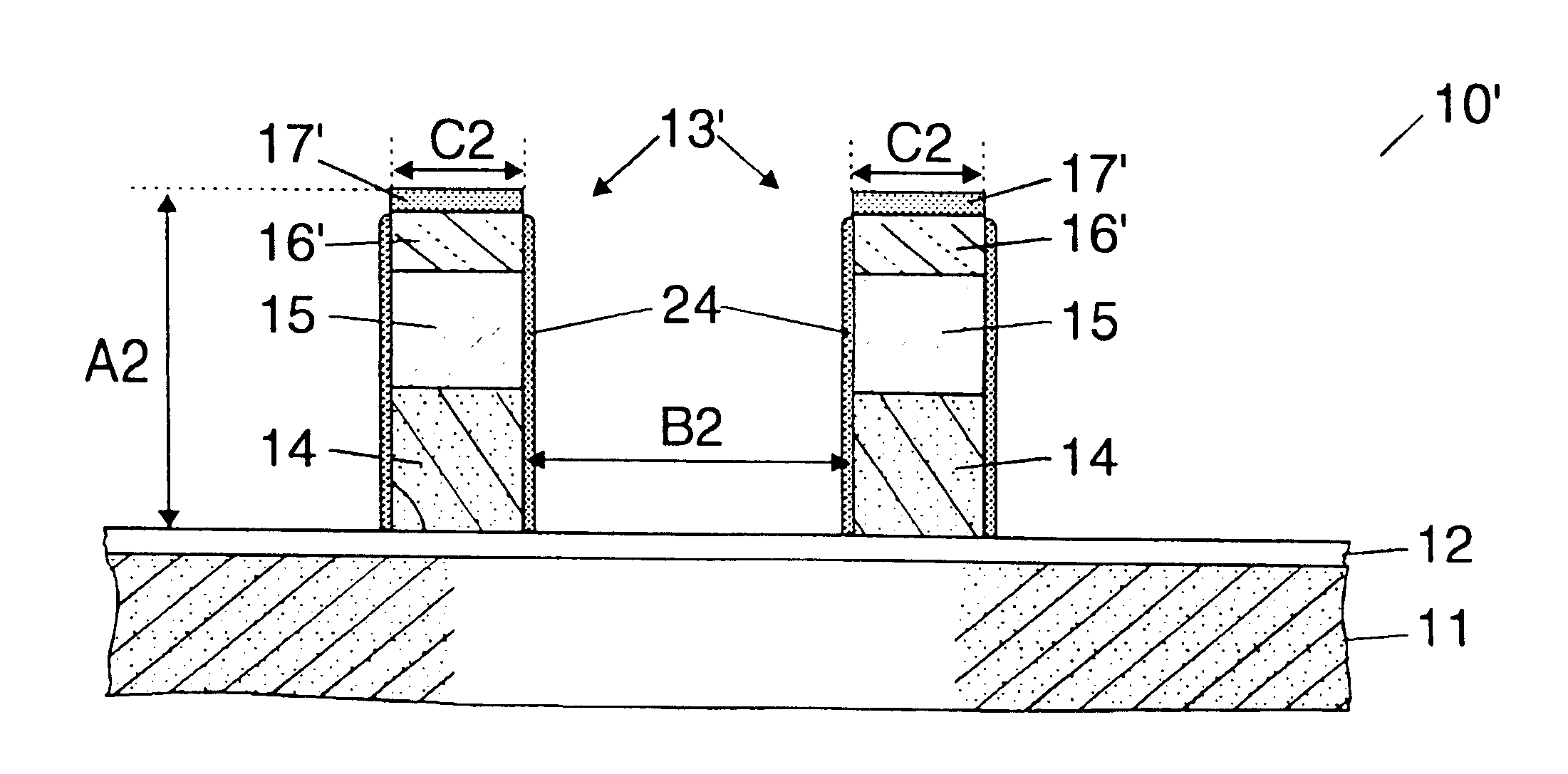
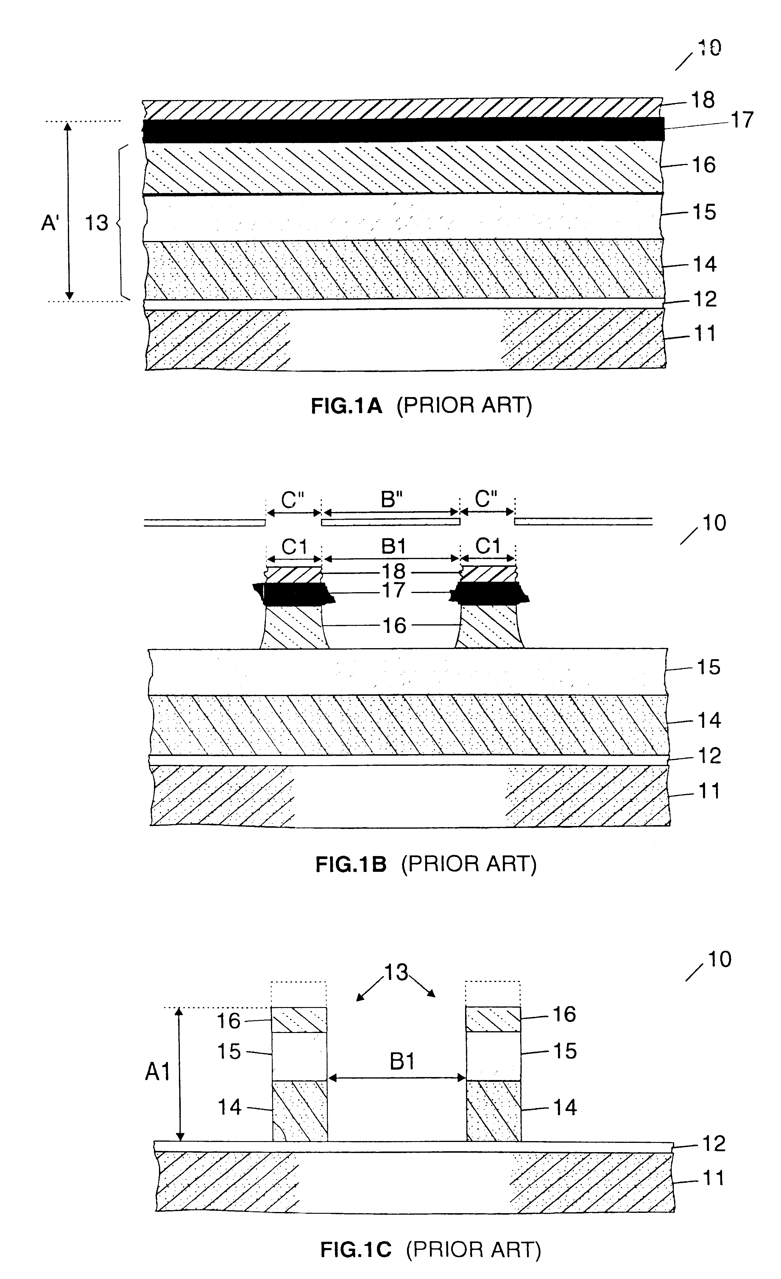
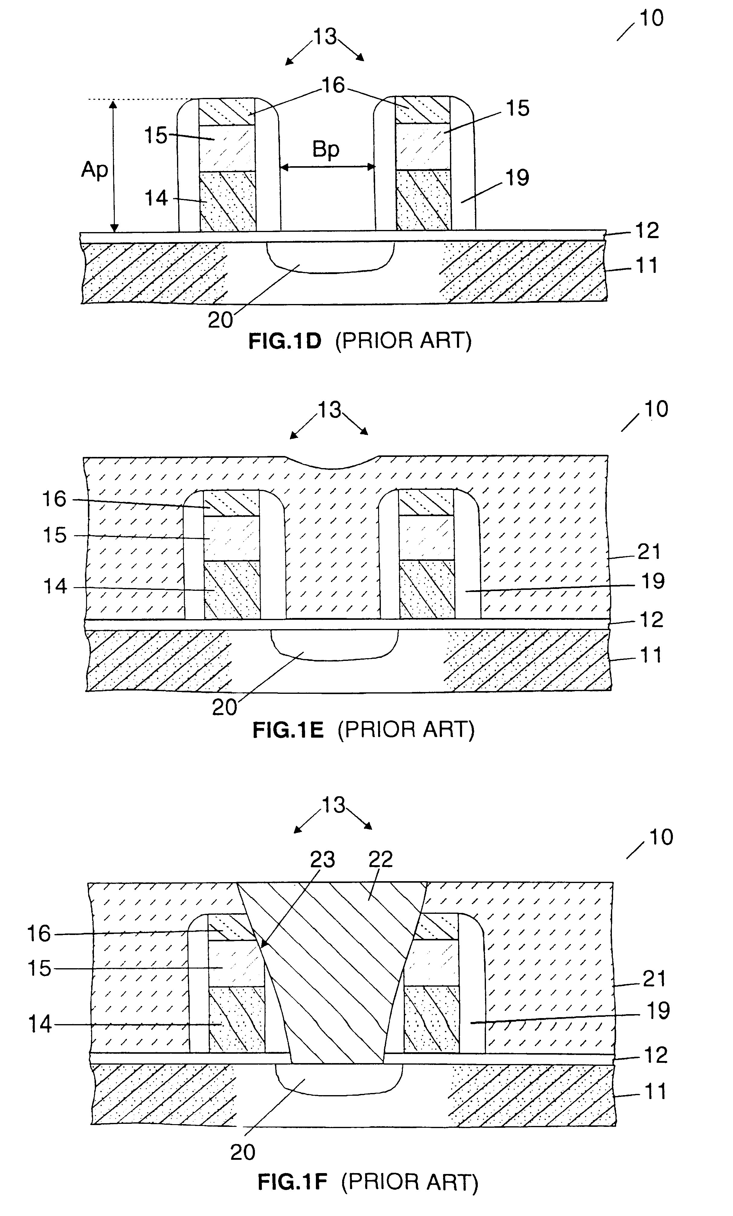
Applicants' inventors have evidenced that most of the above defects were related to the BARL material.

In essence, the main role of the BARL layer 17 is to absorb all incident light emitted by the photo-stepper in order to avoid refractive light induced by the underlying layers (the WSix material has a high reflectance as all metallic films). In reality, it just only allows to improve GC stacks 13 exposure. In substance, it has been pointed out that the BARL material is not impervious enough to UV light. As a result, standing waves caused by unwanted resist exposure due to reflections on the WSix material are created in the resist layer 18, inducing undulations in the resist lines from wafer to wafer and lot to lot with the attendant disadvantages described above.

In the present case of the conventional borderless contact fabrication, the good planarization property of the BARL is rather a drawback. Because, the BARL layer 17 is not conformal at the structure 10 surface, it induces to...


PUM


Abstract

According to the disclosed method, there is provided a structure consisting of a silicon substrate coated with a bottom thin SiO2 layer, a doped polysilicon layer, a refractory metal layer and a top Si3N4 capping layer. Said refractory metal and doped polysilicon layers will form a polycide layer under subsequent thermal treatments. First, a sacrificial layer of a dielectric material such as oxynitride is deposited onto the structure. Oxynitride is impervious to UV radiation and has excellent conformal properties. Then, a layer of a photoresist material is deposited onto the structure and patterned to form a mask. Now the dielectric and top Si3N4 layers are anisotropically etched using the photoresist mask. The mask is stripped and the refractory metal and doped polysilicon layers are anisotropically dry etched down to the SiO2 layer using the patterned dielectric layer as an in-situ hard mask. A conformal layer of Si3N4 is deposited onto the structure, then anisotropically dry etched until the thin SiO2 layer is exposed to form the Si3N4 spacers. Diffusion regions are formed in the substrate by ion implantation. A layer of BPSG is deposited onto the structure and planarized. Contact holes are formed to expose said diffusion regions and filled with a metal to create borderless metal contacts therewith.

Description

The present invention relates to the manufacture of semiconductor integrated circuits and more particularly to an improved method of forming a composite Si3N4 / polycide structure laterally coated with a Si3N4 spacer that has a low aspect ratio. Typically, such a composite structure consists of a top silicon nitride (Si3N4) layer, an intermediate refractory metal silicide layer (e.g. WSix) and a bottom doped polycrystalline silicon (polysilicon) layer. The deposition of a refractory metal silicide over a layer of doped polysilicon is extensively used in the semiconductor industry, forming a so-called polycide layer. The above method finds a valuable application in the fabrication of borderless metal contacts.In the manufacture of such advanced semiconductor IC's, particularly in dynamic random access memory (DRAM) chips, insulated gate field effect transistors (IGFETs) are extensively used. In a particular implementation commonly found in 16 / 64 Mbit DRAM chips, each individual memory ...

Claims


Application Information

Patent Timeline
IPC IPC(8): H01L21/02H01L21/60H01L21/3213
CPCH01L21/76897H01L21/32139H01L21/32137
Inventor CORONEL, PHILIPPECOSTAGANNA, PASCALHEINECK, LARS
Owner IBM CORP
Why Eureka
Try Eureka