Printing one or more electrically conductive bonding lines to provide electrical conductivity in a circuit

a technology of electrical conductivity and bonding lines, applied in the field of circuits, can solve problems such as one or more problems, danger of wire sagging or wire shortage, wires to elements of integrated circuit packages, etc., and achieve the effect of reducing or eliminating the supply of electrical conductivity in a circui

Inactive Publication Date: 2005-03-03
TEXAS INSTR INC
View PDF3 Cites 55 Cited by
  • Summary
  • Abstract
  • Description
  • Claims
  • Application Information

AI Technical Summary

Benefits of technology

[0003] According to the present invention, certain disadvantages and problems associated with previous techniques for providing electrical conductivity in a circuit may be reduced or eliminated.
[0007] Particular embodiments of the present invention may provide one or more technical advantages. In certain embodiments, using the one or more printed electrically conductive bonding lines may allow finer pitch (i.e. center-to-center separation) of bonding lines in an integrated circuit package or other structure relative to using one or more bonding wires. In certain embodiments, problems associated with sagging wire bonds or wire shortages may be reduced or eliminated. For example, in certain embodiments improvements in the quality of connections may occur due to relatively accurate printing technology instead of mechanical wire bonds. In certain embodiments, the time required to produce integrated circuit packages or other structures may be decreased because the time to print the one or more electrically conductive bonding lines may not depend on the number of bonding lines to be printed (as opposed to dependency on the number of wires in previous methods). In certain embodiments, a printer used to print the electrically conductive bonding lines may provide desirable resolution, detail, ultra-fine sizes, and accuracy.

Problems solved by technology

Using wire bonds to connect elements of integrated circuit packages or other structures may result in one or more problems.
For example, there may be a danger of wire sagging or wire shortage as the number of wires increases or the distance between elements connected by wires increases.
As another example, because the time required to bond the wires to the elements of the package or other structure may depend on the number of wires used, bonding the wires to elements of integrated circuit packages and other structures may be a relatively slow process, possibly increasing production time.

Method used


Image

  • Printing one or more electrically conductive bonding lines to provide electrical conductivity in a circuit
  • Printing one or more electrically conductive bonding lines to provide electrical conductivity in a circuit
  • Printing one or more electrically conductive bonding lines to provide electrical conductivity in a circuit

Examples


Embodiment Construction

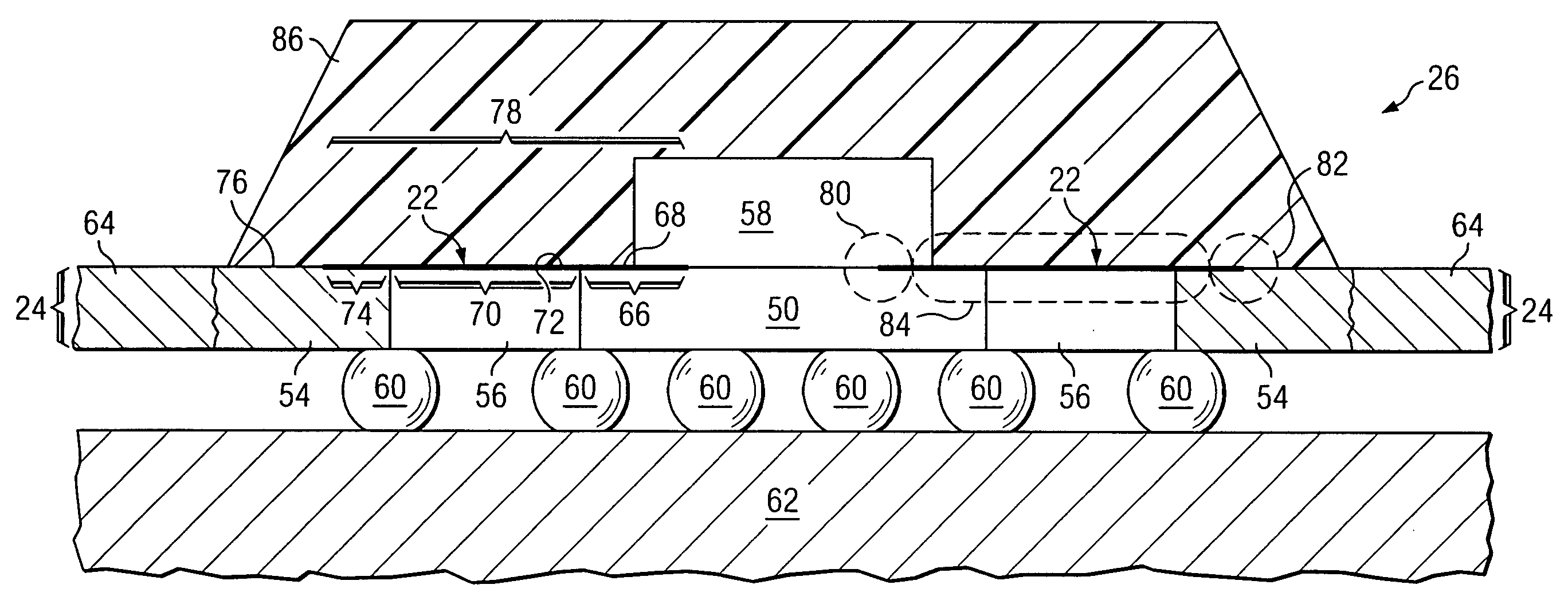
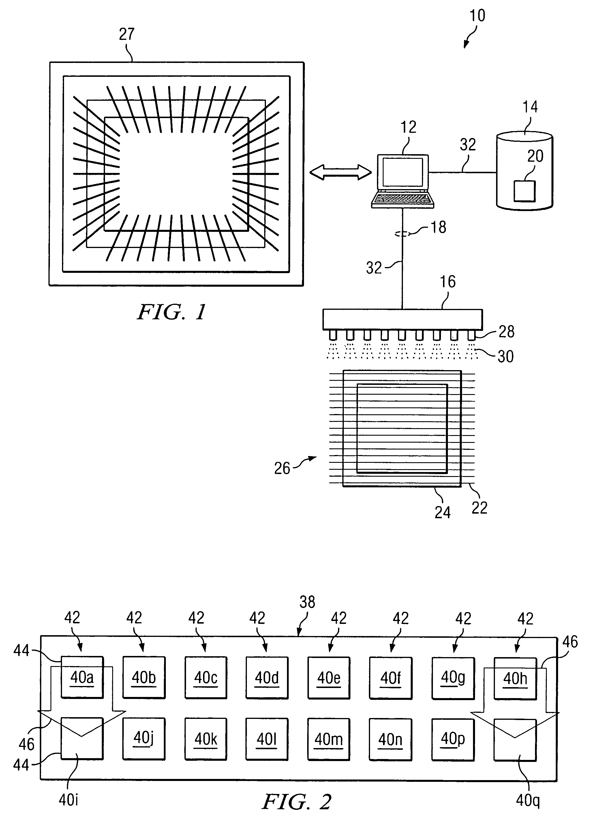
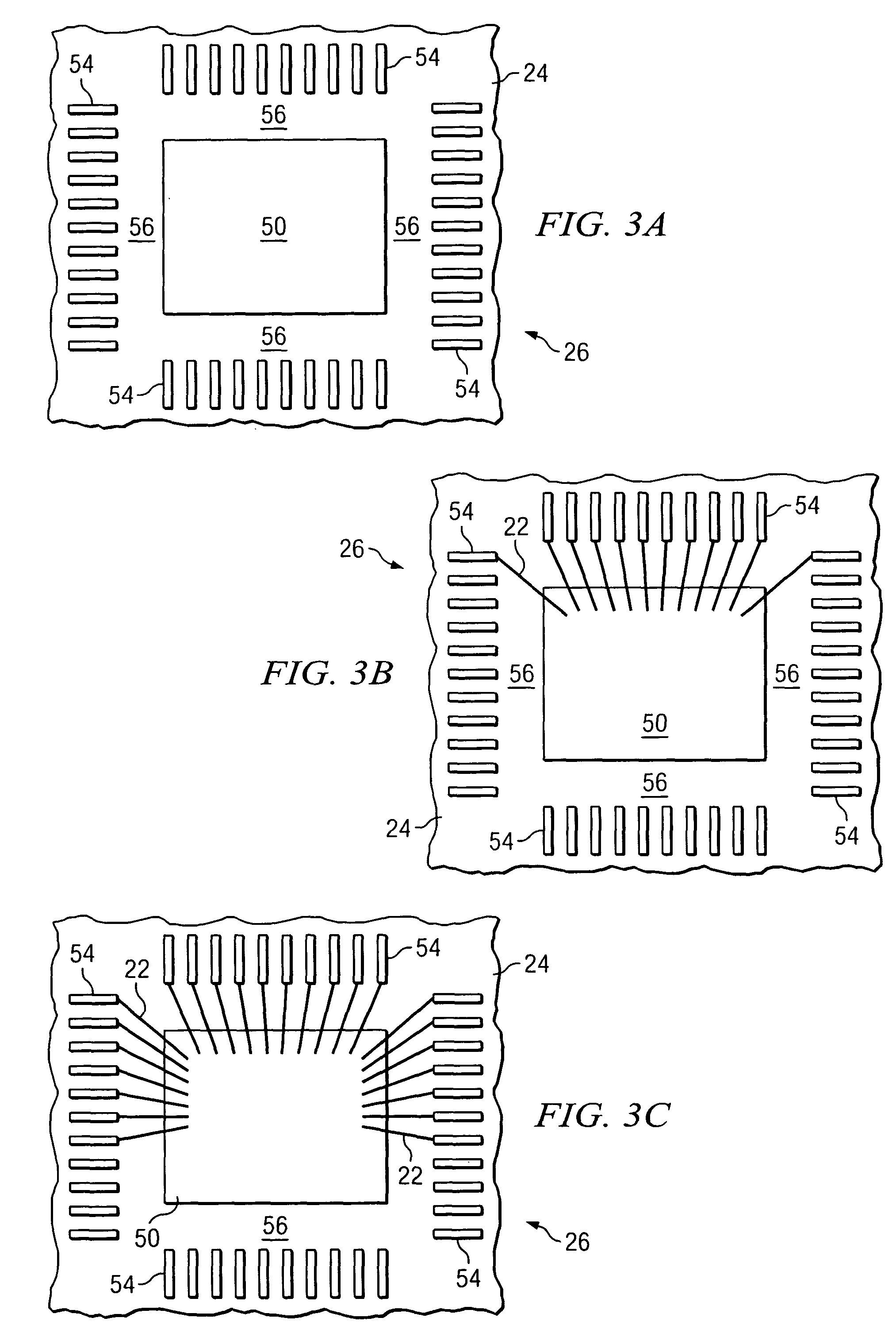
[0015]FIG. 1 illustrates an example system 10 for forming a circuit using one or more electrically conductive bonding lines printed on a substrate. System 10 may comprise a computer system 12, a memory 14, and a printer 16. In general, computer system 12 is operable to generate one or more printing instructions 18 based on bonding data 20 stored in memory 14, and printer 16 is operable to print one or more electrically conductive bonding lines 22 substantially on the surface of a substrate 24 based on printing instructions 18. Electrically conductive bonding lines 22 are operable to provide electrical conductivity between a first element of a circuit 26 and one or more second elements of circuit 26. In one embodiment, electrically conductive bonding lines 22 are used in lieu of standard gold wire bonding.

[0016] Circuit 26 may include an integrated circuit package such as a ball grid array (BGA) type circuit, a leaded package, a printed circuit board package, or any other suitable c...


PUM


Abstract

In one embodiment, a method for forming a circuit comprises generating bonding data specifying locations for one or more electrically conductive bonding lines and generating one or more printing instructions based on the bonding data. The method further comprises, using the printing instructions, printing the one or more electrically conductive bonding lines substantially on a surface of a substrate, the one or more electrically conductive bonding lines operable to provide electrical conductivity between a first element of the circuit and one or more second elements of the circuit.

Description

TECHNICAL FIELD OF THE INVENTION [0001] This invention relates generally to circuits and more particularly to printing one or more electrically conductive bonding lines to provide electrical conductivity in a circuit. BACKGROUND [0002] Integrated circuit packages and other structures such as printed circuit boards generally comprise one or more wire bonds between one or more elements of the structure. For example, an integrated circuit package may comprise one or more gold or other wire bonds that each connect a die associated with the integrated circuit package to one or more leads of the integrated circuit package. Using wire bonds to connect elements of integrated circuit packages or other structures may result in one or more problems. For example, there may be a danger of wire sagging or wire shortage as the number of wires increases or the distance between elements connected by wires increases. As another example, because the time required to bond the wires to the elements of t...

Claims


Application Information

Patent Timeline
Patent Type & Authority Applications(United States)
IPC IPC(8): H01L21/00H01L21/48H01L21/60H01L23/31H01L23/498H01L23/538H05K1/11H05K3/12
CPCH01L23/3128H01L2224/82102H01L23/5389H01L24/18H01L24/81H01L24/82H01L2224/18H01L2224/76155H01L2224/81801H01L2924/01029H01L2924/01079H01L2924/01082H01L2924/14H01L2924/15311H05K1/111H05K3/125H05K2203/013H05K2203/173H01L2924/01033H01L2924/01047H01L2924/014H01L23/49861H01L2924/181H01L2924/12042H01L2224/24175H01L2224/04105H01L2224/32245H01L2224/73267H01L2224/92244H01L24/19H01L2224/24245H01L2924/00
Inventor MATSUNAMI, AKIRA
Owner TEXAS INSTR INC
Why Eureka
Try Eureka