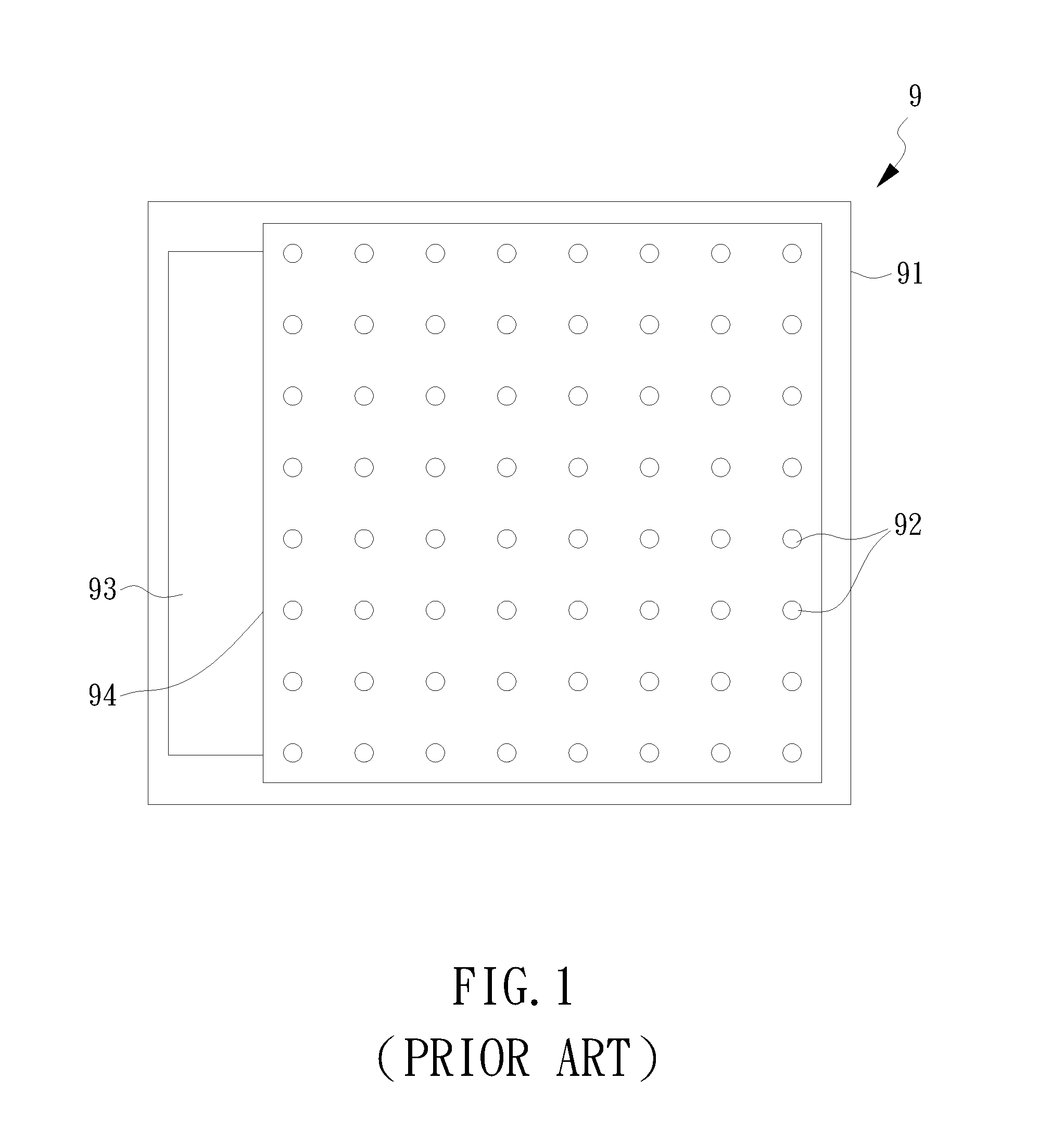
Chip Array Structure for Laser Diodes and Packaging Device for the Device
a laser diode and array structure technology, applied in the direction of lasers, semiconductor lasers, solid-state devices, etc., can solve the problems of inhomogeneous illumination of laser elements, laser chip satisfaction, etc., and achieve the effect of improving uneven power distribution and donut-type illumination pattern
- Summary
- Abstract
- Description
- Claims
- Application Information
AI Technical Summary
Benefits of technology
Problems solved by technology
Method used
Image

Examples
first embodiment
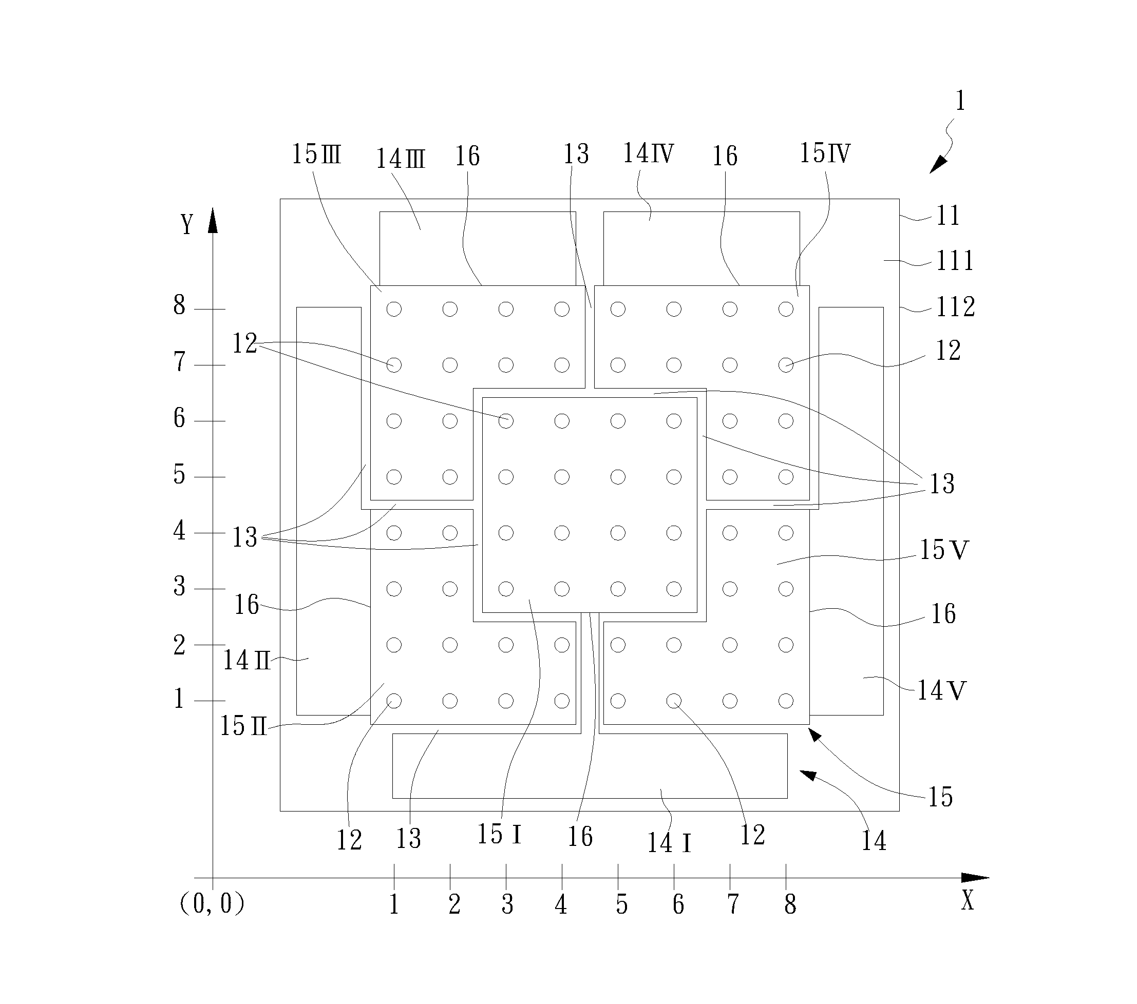
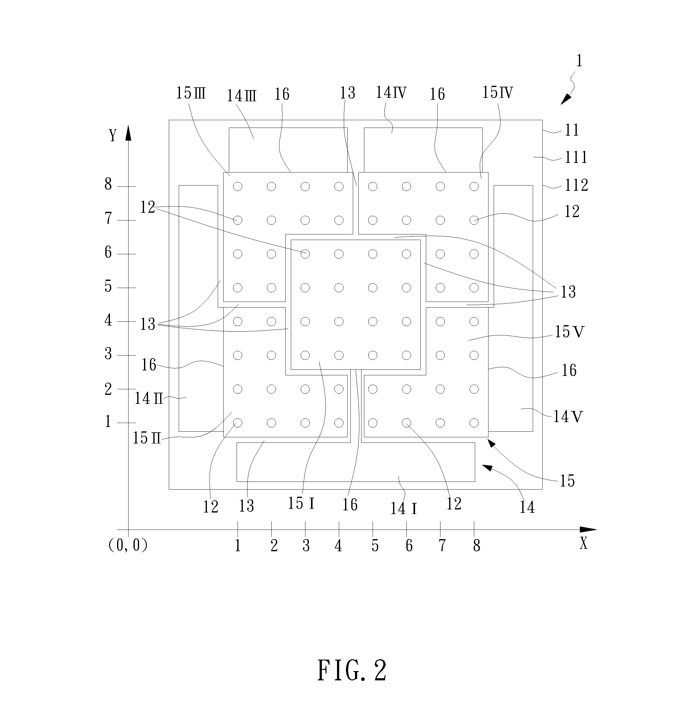
[0024]The semiconductor chip 11 has two opposing surfaces, the active surface 111 and a bottom surface 112. A metal electrode layer is formed on the bottom surface 112, and the polarity (N or P) of the metal electrode layer is opposite to that of the wire bond areas 14 on the active surface 11. In the first embodiment, the wire bond areas 14 are all P welding pads, while the bottom surface 112 is an N electrode.
[0025]In the first embodiment as shown in FIG. 2, the light-emitting elements 12 include 64 elements formed in an 8×8 square array on the active surface 111 of the semiconductor chip 11. The wire bond areas 14 (five shown in this embodiment) are to surround laterally the square array. In another embodiment of the present invention (not shown here), the light-emitting elements 12 can also include 256 elements formed in a 16×16 array. In the present invention, the light-emitting element 12 can be one of the vertical cavity surface emitting Laser (VCSEL), the horizontal cavity s...
second embodiment
[0044]Accordingly, referred to FIG. 3, the light-emitting districts 15aI˜15aVIII of the chip array structure 1a for laser diodes in accordance with the present invention, separated by the insulation wall 13a, can be defined by ranges of corresponding coordinates (x, y) in the X / Y coordinate system as follows.
[0045]Light-emitting district 15aI: (2˜3, 3˜5), (4, 4˜5);
[0046]Light-emitting district 15aII: (5˜6, 4˜6), (7, 4˜5);
[0047]Light-emitting district 15aIII: (1˜4, 1), (1˜3, 2), (1, 3);
[0048]Light-emitting district 15aIV: (1, 4˜8), (1, 6˜8);
[0049]Light-emitting district 15aV: (3˜4, 6˜8), (5, 7˜8);
[0050]Light-emitting district 15aVI: (6, 7˜8), (7˜8, 6˜8);
[0051]Light-emitting district 15aVII: (7, 1˜3), (8, 1˜5); and
[0052]Light-emitting district 15aVIII: (4, 2˜3), (5˜6, 1˜3).
[0053]As illustrated in FIG. 3, the light-emitting districts 15aI and 15aII are surrounded by the other light-emitting districts 15aIII˜15aVIII.
[0054]Also, the light-emitting districts 15aI˜15aVIII are individually,...
third embodiment
[0064]Accordingly, referred to FIG. 4, the light-emitting districts 15bI˜15bIV of the chip array structure 1b for laser diodes in accordance with the present invention, separated by the insulation wall 13b, can be defined by ranges of corresponding coordinates (x, y) in the X / Y coordinate system as follows.
[0065]Light-emitting district 15bI: (3˜4,4˜6), (5,3˜6), (6,3˜8);
[0066]Light-emitting district 15bII: (1˜6,1˜2), (1˜4,3);
[0067]Light-emitting district 15bIII: (1˜2,4˜8), (3˜5,7˜8); and
[0068]Light-emitting district 15bIV: (7˜8, 1˜8).
[0069]As illustrated in FIG. 4, the light-emitting districts 15bI is largely surrounded by the other light-emitting districts 15bII˜15bIV. Also, the light-emitting districts 15bI˜15bIV are individually, in an electric independence way, connected to the corresponding wire bond areas 14bI˜14bIV whom are also electrically isolated from each other. As shown, the locations of the wire bond areas 14bI˜14bIV with respect to the array of the light-emitting eleme...
PUM
 Abstract
Description
Claims
Application Information
 - R&D
- Intellectual Property
- Life Sciences
- Materials
- Tech Scout
- Unparalleled Data Quality
- Higher Quality Content
- 60% Fewer Hallucinations
Browse by: Latest US Patents, China's latest patents, Technical Efficacy Thesaurus, Application Domain, Technology Topic, Popular Technical Reports.
© 2025 PatSnap. All rights reserved.Legal|Privacy policy|Modern Slavery Act Transparency Statement|Sitemap|About US| Contact US: help@patsnap.com