Semiconductor device and method for manufacturing the same

a semiconductor device and semiconductor technology, applied in semiconductor devices, semiconductor/solid-state device details, electrical devices, etc., can solve the problems of increasing the thermal resistance of the semiconductor device, and increasing the loss of the semiconductor device in the circuit portion

Active Publication Date: 2015-03-26
MITSUBISHI ELECTRIC CORP
View PDF3 Cites 14 Cited by
  • Summary
  • Abstract
  • Description
  • Claims
  • Application Information

AI Technical Summary

Benefits of technology

[0005]In a conventional semiconductor device, a Si substrate having a thickness of about 100 μm exists below a transistor portion, a pad portion, a wiring portion and a passive circuit portion, with a several micrometer-thick epitaxial layer interposed therebetween, the epitaxial layer comprising GaN or AlGaN. Even the resistivity of a high resistance type of Si substrate is about 104 Ωcm, which is four to five orders of magnitude lower than those of semi-insulating GaAs substrates and SiC substrates used in high-frequency-band semiconductor devices. The conductor loss in a circuit portion is increased thereby.

Problems solved by technology

The conductor loss in a circuit portion is increased thereby.
Therefore, heat generated in a transistor in such a semiconductor device cannot easily be released, and the thermal resistance of the semiconductor device is increased.
In the case of use of the semiconductor device as a high-output amplifier in particular, the junction temperature is increased during operation, resulting in a reduction in reliability.
However, the lattice constants of the epitaxially grown crystal layer and the filler differ from each other and a defect can occur.
It is, therefore, difficult to deposit the filler.

Method used


Image

  • Semiconductor device and method for manufacturing the same
  • Semiconductor device and method for manufacturing the same
  • Semiconductor device and method for manufacturing the same

Examples


first embodiment

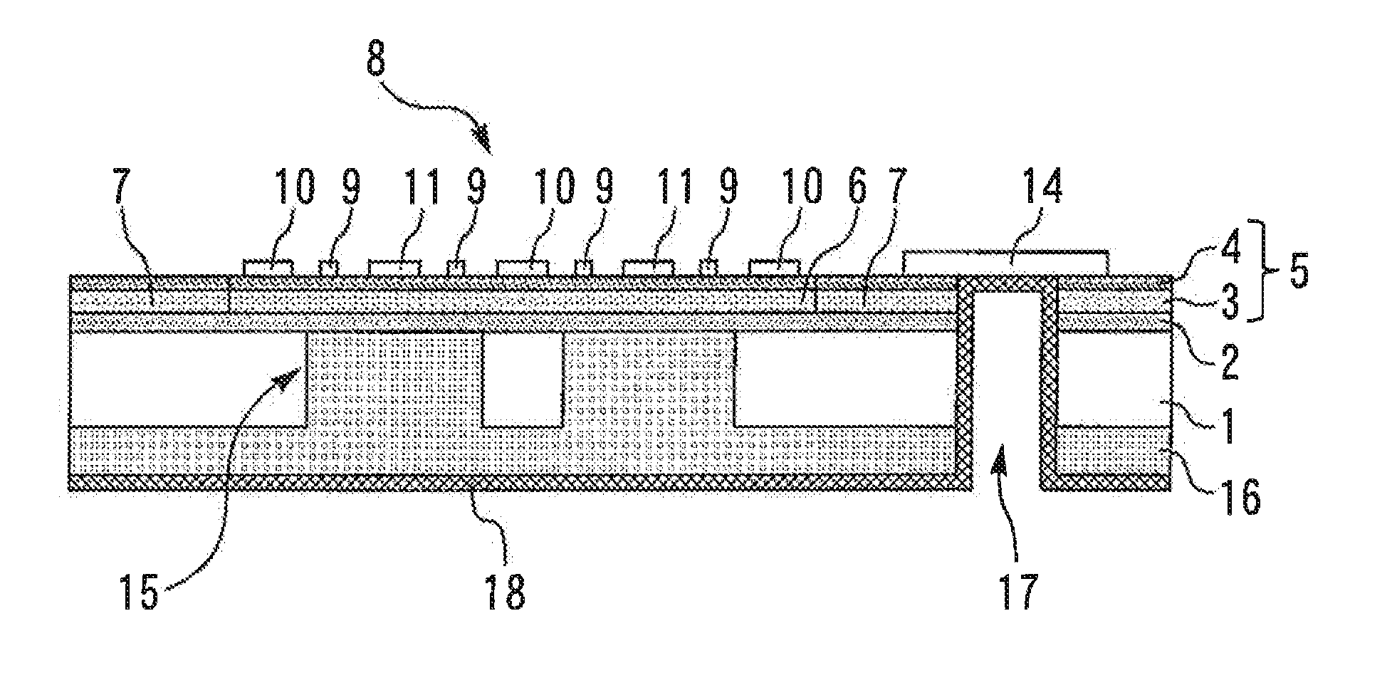
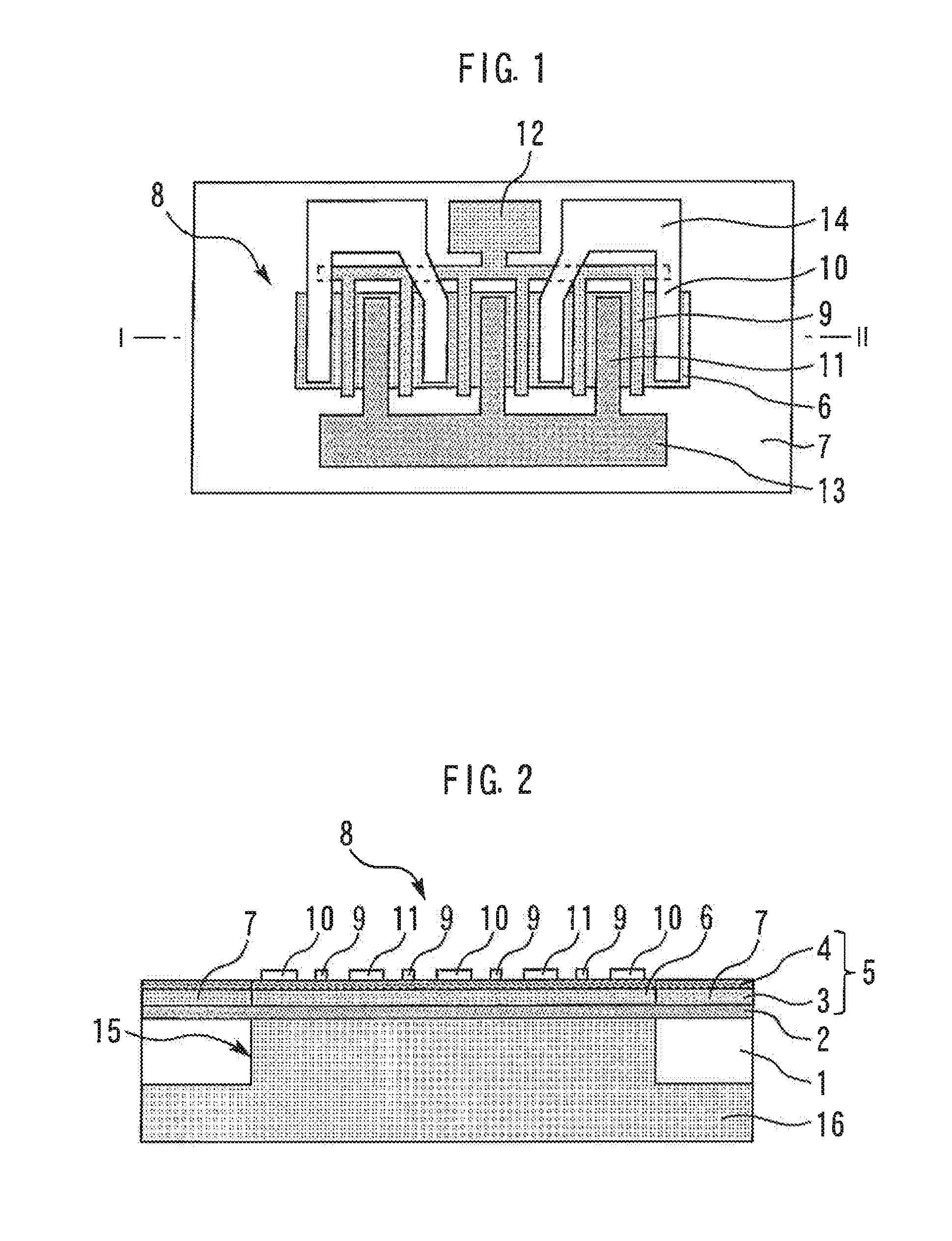
[0022]FIG. 1 is a top view of a semiconductor device according to a first embodiment of the present invention. FIG. 2 is a sectional view taken along line I-II in FIG. 1. A Si substrate 1 has first and second major surfaces facing in opposite directions. A buffer layer 2 formed of AlN is uniformly formed over the entire area of the first major surface of the Si substrate 1. An epitaxially grown crystal layer 5 including a GaN layer 3 and an AlGaN layer 4 laid one on another is formed on the buffer layer 2.

[0023]An active layer region 6 is formed in a portion of the epitaxially grown crystal layer 5, and an insulation region 7 is formed around the active layer region 6 by insulation injection or the like. A transistor 8 is formed in the epitaxially grown crystal layer 5. More specifically, a pair of field-effect transistors having gate electrodes 9, source electrodes 10 and drain electrodes 11 are disposed parallel to each other on the active layer region 6, each gate electrode 9 bei...

second embodiment

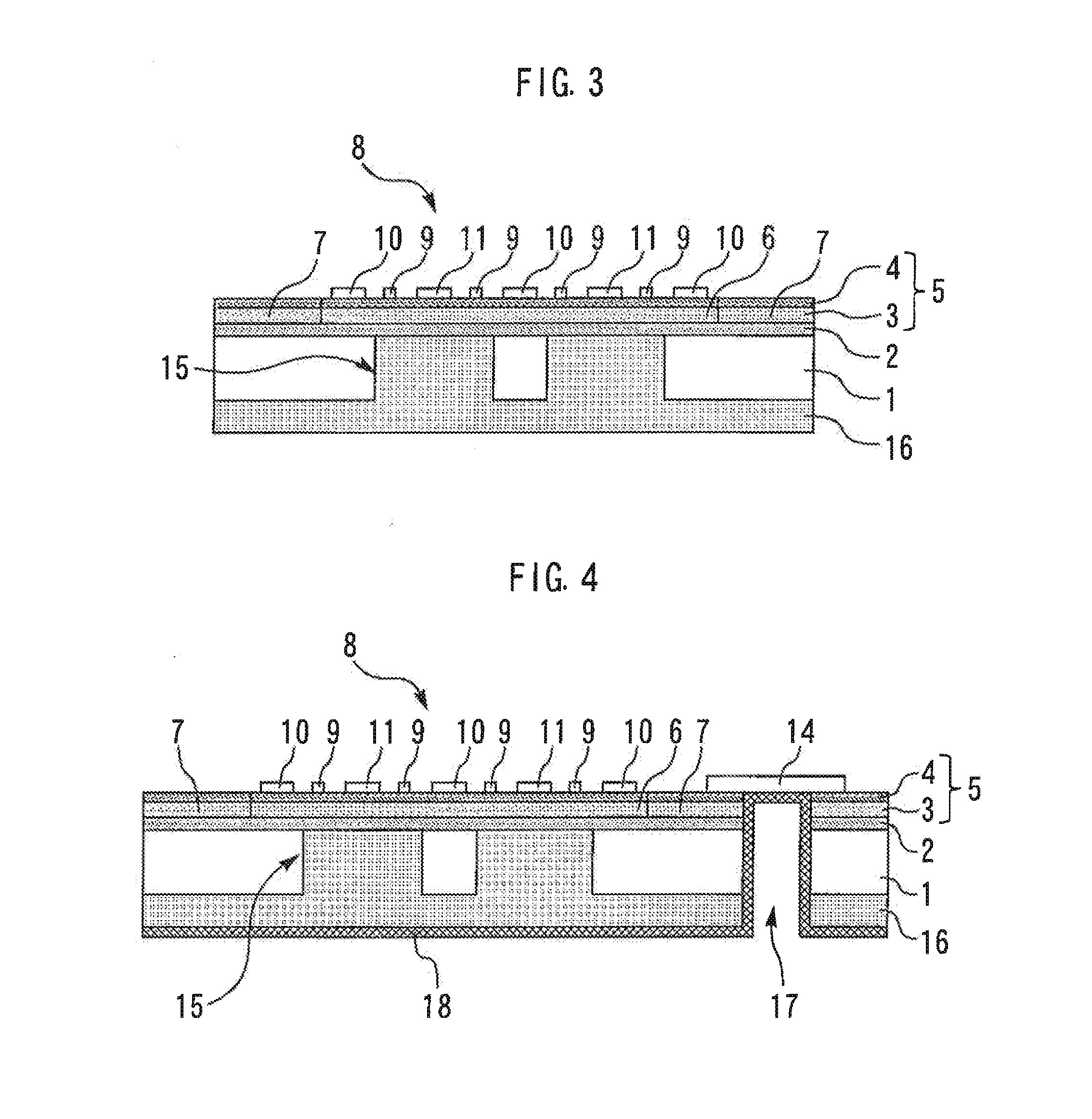
[0032]FIG. 3 is a sectional view of a semiconductor device according to a second embodiment of the present invention. In the present embodiment, the through hole 15 and the filler 16 are provided below the drain electrodes 11 of the transistor 8 but not provided below the source electrodes 10.

[0033]Since an increase in the capacitance Cds between the drain electrodes 11 and the substrate back surface is a cause of degradation of high-frequency characteristics, part of the Si substrate 1 below the drain electrodes 11 may be removed and replaced with the filler 16. The high-frequency characteristics can be improved thereby, as are those in the first embodiment. While the thickness of the AlN layer deposited as filler 16 is about several micrometers in the first embodiment, the thickness of the AlN layer in the present embodiment can be reduced relative to that in the first embodiment. Forming of the filler 16 is facilitated thereby.

third embodiment

[0034]FIG. 4 is a sectional view of a semiconductor device according to a third embodiment of the present invention. A source via hole 17 reaching from the second major surface of the Si substrate 1 to the source pad 14 of the transistor 8 is provided in the insulation region 7. A metal film 18 such as Au plating is provided on the inner wall surface of the source via hole 17 and the second major surface of the Si substrate 1 and is connected to the source pad 14. The distance to a grounding point can be reduced by the metal film 18. The source inductance can thus be reduced to improve the high-frequency characteristics.


PUM


Abstract

A semiconductor device includes: a Si substrate having first and second major surfaces facing in opposite directions; a buffer layer of AlxGa1-xN (0≦x≦1) on the first major surface of the Si substrate; an epitaxially grown crystalline layer of AlyGa1-yN (0≦y≦1, x≠y) on the buffer layer; a transistor on the epitaxially grown crystalline layer; and a filler of AlxGa1-xN and having the same x as the buffer layer. A through hole in the Si substrate extends from the second major surface to the buffer layer, and the through hole is filled with the filler.

Description

BACKGROUND OF THE INVENTION[0001]1. Field of the Invention[0002]The present invention relates to a field effect transistor formed in an epitaxially grown crystal layer formed of GaN or AlGaN on a Si substrate, and a MMIC including the field effect transistor.[0003]2. Background Art[0004]A semiconductor device is known in which an epitaxially grown crystal layer formed of GaN or AlGaN is formed on a Si substrate, and in which a field effect transistor is formed in the epitaxially grown crystal layer (see, for example, Japanese patent Laid-Open Nos. 2009-206142 and 2010-67662).SUMMARY OF THE INVENTION[0005]In a conventional semiconductor device, a Si substrate having a thickness of about 100 μm exists below a transistor portion, a pad portion, a wiring portion and a passive circuit portion, with a several micrometer-thick epitaxial layer interposed therebetween, the epitaxial layer comprising GaN or AlGaN. Even the resistivity of a high resistance type of Si substrate is about 104 Ωcm...

Claims


Application Information

Patent Timeline
Patent Type & Authority Applications(United States)
IPC IPC(8): H01L29/78H01L29/66
CPCH01L29/66522H01L29/78H01L29/2003H01L29/4175H01L29/41758H01L29/42316H01L29/7787H01L23/3677H01L29/7786H01L29/0657H01L2924/0002H01L2924/00H01L29/7843H01L29/7849
Inventor OKAZAKI, HIROYUKIKAMO, YOSHITAKANOGAMI, YOICHIKOYAMA, HIDETOSHIMIYAKUNI, SHINICHI
Owner MITSUBISHI ELECTRIC CORP
Why Eureka
Try Eureka