Electronic component and method for manufacturing the same

a technology of electronic components and manufacturing methods, applied in the field of electronic components, can solve problems such as deterioration of electrical characteristics of electronic components

Active Publication Date: 2015-03-26
MURATA MFG CO LTD
View PDF1 Cites 41 Cited by
  • Summary
  • Abstract
  • Description
  • Claims
  • Application Information

AI Technical Summary

Benefits of technology

[0023]According to various preferred embodiments of the present invention, an occurrence of a crack in an element...

Problems solved by technology

As described above, in the case where a crack is generated in an electronic component by tensile stress due to th...

Method used


Image

  • Electronic component and method for manufacturing the same
  • Electronic component and method for manufacturing the same
  • Electronic component and method for manufacturing the same

Examples


first preferred embodiment

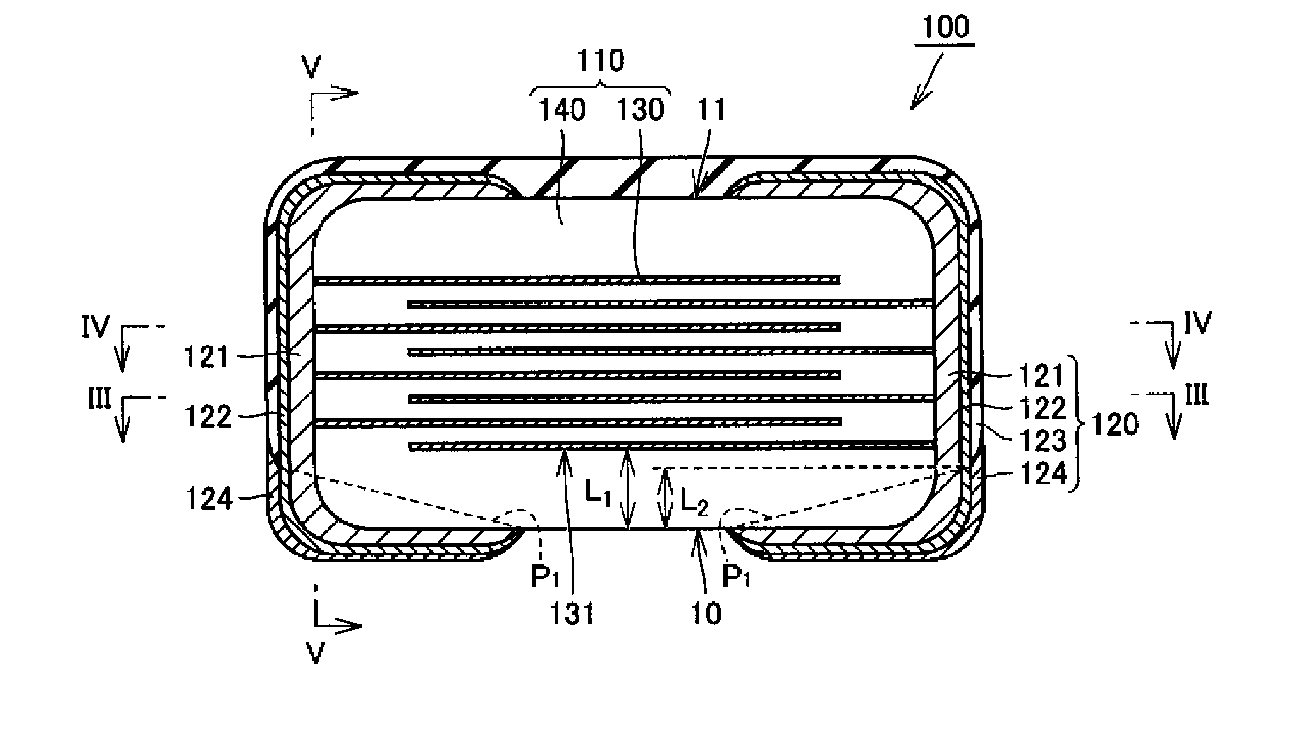
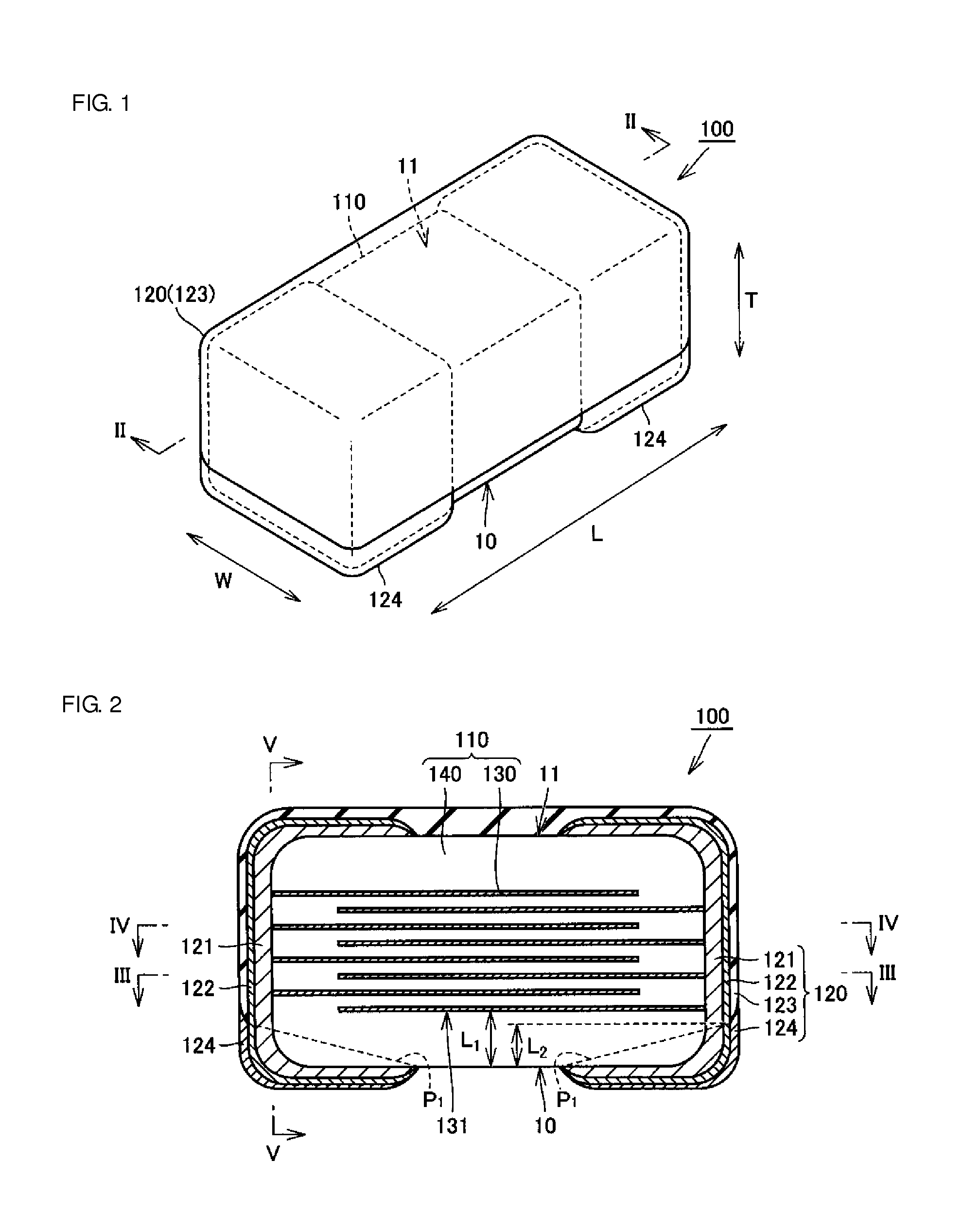
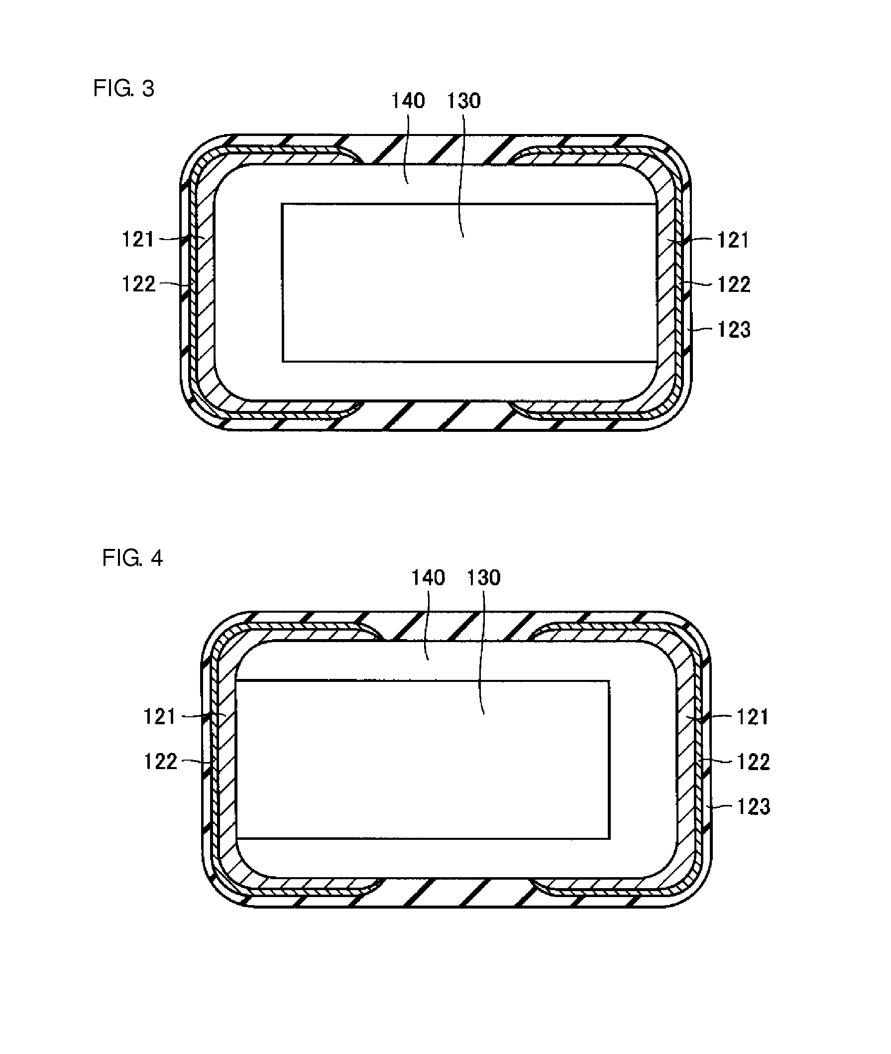
[0044]FIG. 1 is a perspective view illustrating an external appearance of an electronic component according to a first preferred embodiment of the present invention. FIG. 2 is a cross-sectional view of the electronic component taken along a II-II arrow line in FIG. 1. FIG. 3 is a cross-sectional view of the electronic component taken along a III-III arrow line in FIG. 2. FIG. 4 is a cross-sectional view of the electronic component taken along a IV-IV arrow line in FIG. 2. FIG. 5 is a cross-sectional view of the electronic component taken along a V-V arrow line in FIG. 2. In FIG. 1, a lengthwise direction of an element assembly, which will be explained later in detail, is indicated by “L”, a width direction of the element assembly is indicated by “W”, and a thickness direction of the element assembly is indicated by “T”.

[0045]As shown in FIGS. 1 through 5, an electronic component 100 according to the first preferred embodiment of the present invention includes a parallelepiped-shaped...

second preferred embodiment

[0124]FIG. 8 is a cross-sectional view illustrating a configuration of the electronic component according to the second preferred embodiment of the present invention. FIG. 9 is a flowchart illustrating a method for manufacturing the electronic component according to the second preferred embodiment of the present invention. Note that FIG. 8 illustrates a cross section of the electronic component viewed from the same direction as in FIG. 2.

[0125]As shown in FIG. 8, an outer electrode 120a of the electronic component 100a according to the second preferred embodiment of the present invention further includes a base layer 125 which is made of a material different from that of the reinforcement layer 122 and contains Cu or Ni. The base layer 125 is provided between the sintered layer 121 and the reinforcement layer 122 so as to cover the entirety of the sintered layer 121.

[0126]The base layer 125 is directly provided on the sintered layer 121 so as to cover the entirety of the sintered la...

third preferred embodiment

[0137]FIG. 10 is a cross-sectional view illustrating a configuration of the electronic component according to the third preferred embodiment of the present invention. FIG. 11 is a flowchart illustrating a method for manufacturing the electronic component according to the third preferred embodiment of the present invention. Note that FIG. 10 illustrates a cross section of the electronic component viewed from the same direction as in FIG. 2.

[0138]As shown in FIG. 10, an outer electrode 120b of the electronic component 100b according to the third preferred embodiment of the present invention further includes a shield layer 126 configured of a material different from that of the reinforcement layer 122 and containing Cu or Ni. The shield layer 126 is provided between the reinforcement layer 122 and the Sn-containing layer 124.

[0139]The shield layer 126 is provided on the reinforcement layer 122 so as to cover the reinforcement layer 122 except for a portion of the reinforcement layer 12...


PUM

PropertyMeasurementUnit
Timeaaaaaaaaaa
Distanceaaaaaaaaaa

Abstract

In an electronic component, an outer electrode includes a sintered layer including a sintered metal, a reinforcement layer not containing Sn but including Cu or Ni, an insulation layer, and a Sn-containing layer. The sintered layer extends from each end surface of an element assembly onto at least one main surface thereof to cover each end surface of the element assembly. The reinforcement layer extends on the sintered layer and covers the sintered layer entirely. The insulation layer is directly provided on the reinforcement layer at each end surface of the element assembly, extends in a direction perpendicular or substantially perpendicular to a side surface of the element assembly, and defines a portion of a surface of the outer electrode. The Sn-containing layer covers the reinforcement layer except for a portion of the reinforcement layer that is covered by the insulation layer, and defines another portion of the surface of the outer electrode.

Description

BACKGROUND OF THE INVENTION[0001]1. Field of the Invention[0002]The present invention relates to electronic components and methods for manufacturing the electronic components, specifically to electronic components mounted by soldering and methods for manufacturing the electronic components.[0003]2. Description of the Related Art[0004]Japanese Unexamined Patent Application Publication No. 2003-22929 describes a multilayer ceramic capacitor in which an occurrence of a short circuit of inner electrodes due to a crack generated by thermal contraction of a solder fillet is suppressed.[0005]In the multilayer ceramic capacitor disclosed in Japanese Unexamined Patent Application Publication No. 2003-22929, in the case where a crack is generated in an element assembly in the vicinity of one outer electrode thereof by tension of a solder fillet, inner electrodes connected to the other outer electrode are prevented from being exposed in a gap of the crack. This suppresses the occurrence of a s...

Claims


Application Information

Patent Timeline
IPC IPC(8): H01C7/00H01F27/28H01G4/30H01G4/008H01L41/047H01L41/083
CPCH01C7/008H01L41/0477H01L41/083H01F2027/2809H01G4/008H01F27/2804H01G4/30H01G4/232H01F17/0013H01F27/292Y10T29/42Y10T29/49206H10N30/872H10N30/877H01G4/248Y10T29/43Y10T29/435
Inventor MORI, HARUHIKOOTSUNA, HIROYUKI
Owner MURATA MFG CO LTD
Why Eureka
Try Eureka