This helps you quickly interpret patents by identifying the three key elements:
Problems solved by technology
Method used
Benefits of technology
Benefits of technology
[0006]In a semiconductor device having an integrated circuit provided on a semiconductor substrate thereof, a plurality of electrode pads are provided on the semiconductor substrate and, therefore, has limitation in wiring design rule, unlike in a semiconductor device including discrete components. That is, where one of the electrode pads has an increased size, the other electrode pads should be provided in a region of the semiconductor substrate in which the one electrode pad is absent. Therefore, the routing of wirings connected to the e
Problems solved by technology
In a semiconductor device having an integrated circuit provided on a semiconductor substrate thereof, a plurality of electrode pads are provided o
Method used
Image
Click on the blue label to locate the original text in one second.
Reading with bidirectional positioning of images and text.
Examples
Example
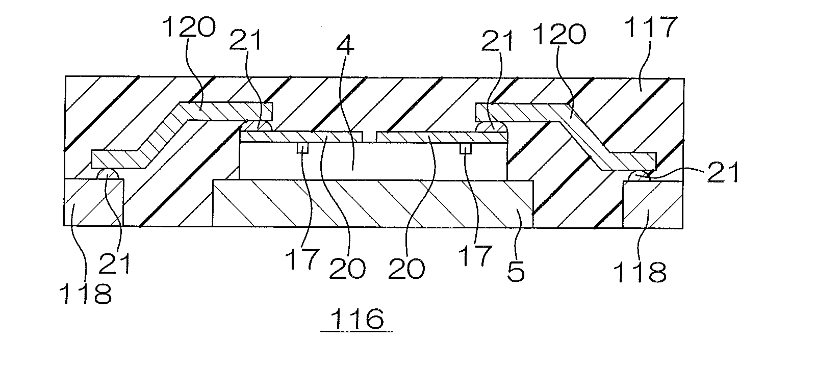
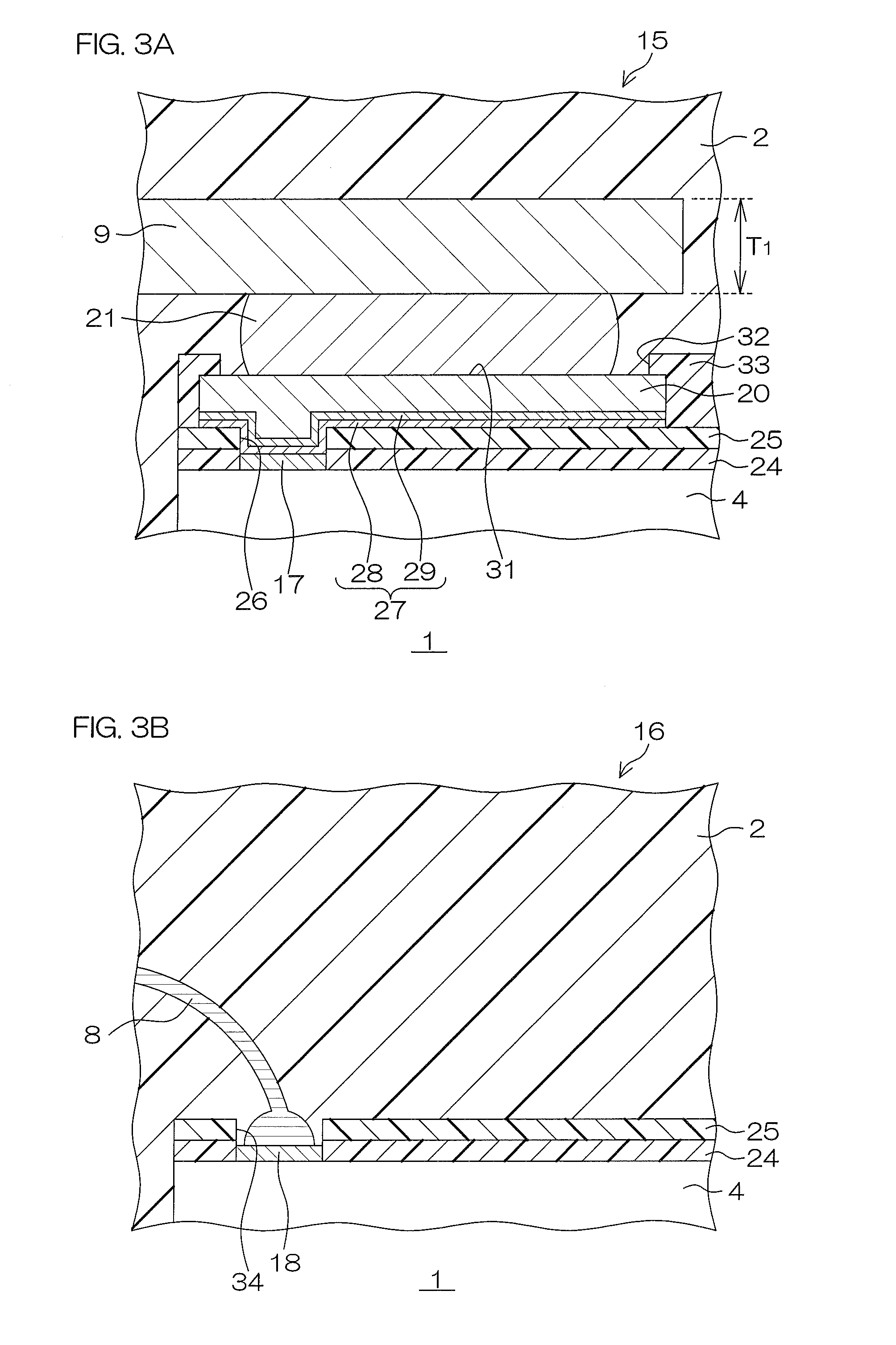
[0105]FIG. 5 is a schematic enlarged sectional view showing a wiring region 15 of a semiconductor device 41 according to a second embodiment of the present invention.
[0106]The semiconductor device 41 of the second embodiment differs from the semiconductor device 1 of the first embodiment in that metal plating films 42 are respectively provided on the wiring pads 31. Except for this arrangement, the semiconductor device 41 has substantially the same construction as the semiconductor device 1 of the first embodiment. In FIG. 5, components corresponding to those shown in FIGS. 1 to 4F are designated by the same reference characters as in FIGS. 1 to 4F, and duplicate description will be omitted.
[0107]The metal plating films 42 respectively cover the surfaces of the wiring pads 31 in the wiring pad openings 32. The metal plating films 42 each have a double layer structure including two layers made of different metal materials. The metal plating films 42 each have a Pd plating film 43 con...
Example
[0112]The semiconductor device 47 of the third embodiment differs from the semiconductor device 1 of the first embodiment in that the clips 9 are connected to the inner lead portions 6 via metal frames 49, and that a plurality of posts 50 are provided on each of the wiring pads 31. Except for this arrangement, the semiconductor device 47 has substantially the same construction as the semiconductor device 1 of the first embodiment. In FIGS. 6 and 7, components corresponding to those shown in FIGS. 1 to 5 are designated by the same reference characters as in FIGS. 1 to 5, and duplicate description will be omitted.
[0113]In this embodiment, as shown in FIG. 6, the metal frames 49, which are made of the same material as the clips 9, are selectively connected to the inner lead portions 6. The metal frames 49 extend along edges of the semiconductor chip 4 to project from some of the leads 3. That is, the metal frames 49 are extensions of the leads 3 extending along the edges of the semicon...
Example
[0129]FIG. 9 is a schematic enlarged sectional view showing a wiring region of a semiconductor device 55 according to a fourth embodiment of the present invention.
[0130]The semiconductor device 55 of the fourth embodiment differs from the semiconductor device 47 of the third embodiment in that metal plating films 56 cover the wiring pads 31 and the posts 50. Except for this arrangement, the semiconductor device 55 has substantially the same construction as the semiconductor device 47 of the third embodiment. In FIG. 9, components corresponding to those shown in FIGS. 1 to 8D are designated by the same reference characters as in FIGS. 1 to 8D, and duplicate description will be omitted.
[0131]The metal plating films 56 of the semiconductor device 55 each have the same structure as the metal plating films 42 of the second embodiment. The metal plating films 56 are formed through the following step. The step of forming a Pd plating film 43 and a Ni plating film 44 to selectively cover th...
PUM
Abstract
An inventive semiconductor device includes: a semiconductor chip including an integrated circuit; a plurality of electrode pads provided on the semiconductor chip and connected to the integrated circuit; a rewiring to which the electrode pads are electrically connected together, the rewiring being exposed on an outermost surface of the semiconductor chip and having an exposed surface area greater than the total area of the electrode pads; and a resin package which seals the semiconductor chip.
Description
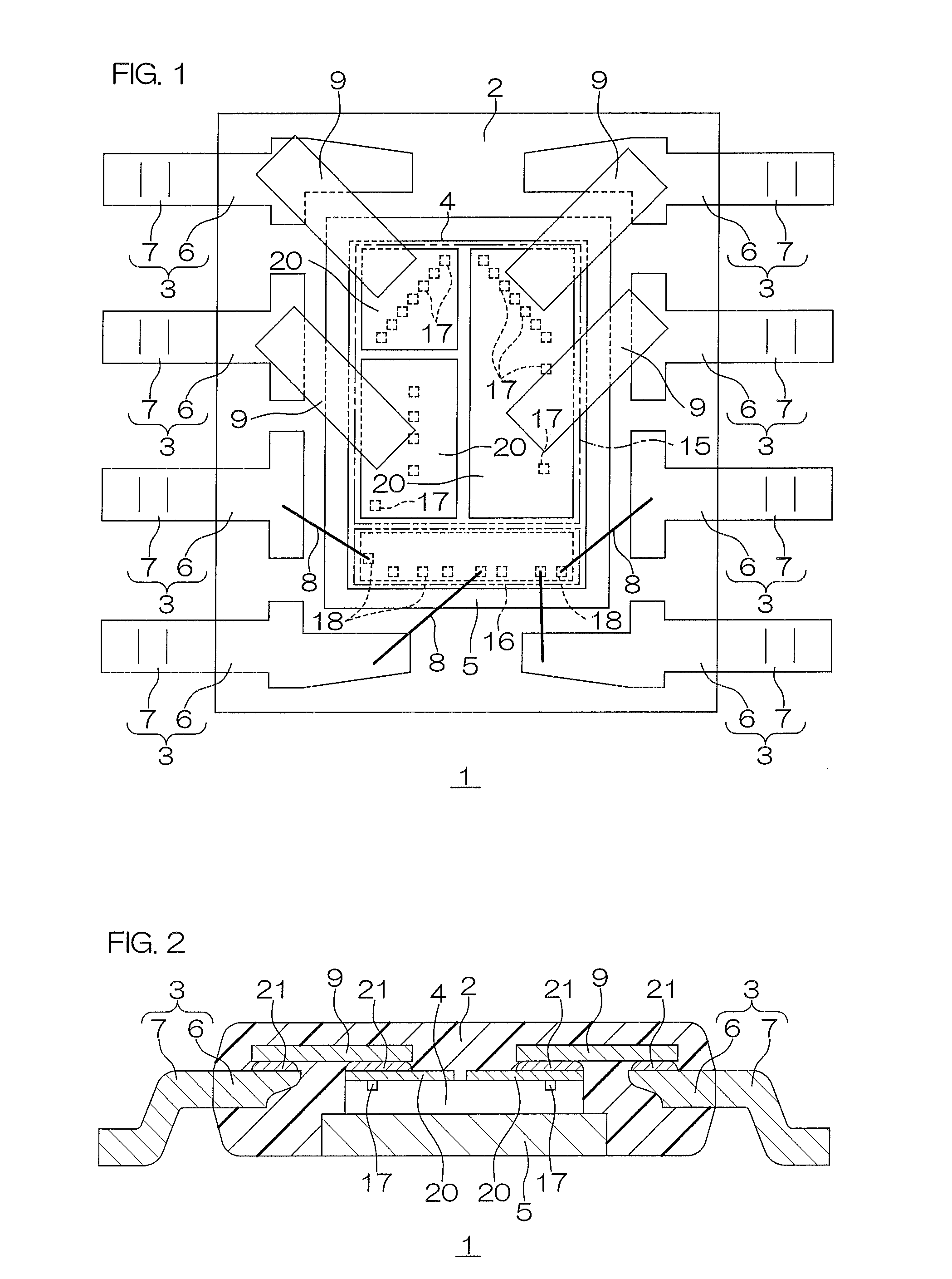
CROSS-REFERENCE TO RELATED APPLICATIONS[0001]This application corresponds to Japanese Patent Application No. 2013-206560 filed in the Japan Patent Office on Oct. 1, 2013, the disclosure of which is incorporated herein by reference in its entirety.FIELD OF THE INVENTION[0002]The present invention relates to a semiconductor device including an integrated circuit.BACKGROUND ART[0003]Patent Document 1 (JP2013-115054A) discloses a semiconductor chip which includes a semiconductor substrate having a front surface formed with a plurality of semiconductor elements, an interlevel insulation film provided on the semiconductor substrate, a plurality of electrode pads provided on the interlevel insulation film, and a surface protection film provided on the interlevel insulation film and having pad openings through which the electrode pads are respectively exposed. The electrode pads are respectively connected to bonding wires in a resin package.BRIEF SUMMARY OF THE INVENTION[0004]With recent hi...
Claims
Application Information
Patent Timeline
Application Date:The date an application was filed.
Publication Date:The date a patent or application was officially published.
First Publication Date:The earliest publication date of a patent with the same application number.
Issue Date:Publication date of the patent grant document.
PCT Entry Date:The Entry date of PCT National Phase.
Estimated Expiry Date:The statutory expiry date of a patent right according to the Patent Law, and it is the longest term of protection that the patent right can achieve without the termination of the patent right due to other reasons(Term extension factor has been taken into account ).
Invalid Date:Actual expiry date is based on effective date or publication date of legal transaction data of invalid patent.
