Integrated circuit and manufacturing method of copper germanide and copper silicide as copper capping layer

a manufacturing method and copper silicide technology, applied in the direction of electrical apparatus, semiconductor device details, semiconductor/solid-state device details, etc., can solve the problems of copper silicide em and stress migration reliability problems, copper silicide formation process conventional drawbacks, and copper silicide may still break from copper silicide and diffuse into low-k dielectric layer

Active Publication Date: 2010-12-28
TAIWAN SEMICON MFG CO LTD +1
View PDF14 Cites 327 Cited by
  • Summary
  • Abstract
  • Description
  • Claims
  • Application Information

AI Technical Summary

Benefits of technology

[0011]The conflicting requirements and needs for a suitable capping layer requires the need for a new capping layer composition as well as an improved method to provide a suitable capping layer which avoids e.g. damage to the surrounding dielectric material(s).
[0012]A novel capping composition should be such that it combines good barrier performance (avoiding Cu out diffusing), low resistivity and stability of the capping layer with acceptable (low) sheet resistance increase.
[0013]A method is provided for obtaining at least one selective capping layer on Cu interconnect structures whereby the capping layer has improved electro-migration (EM) resistance and in combination therewith good barrier performance and acceptable and stable metal sheet resistance (Rs).

Problems solved by technology

However, copper suffers from electro-migration (EM) and stress-migration (SM) reliability issues, particularly as geometries continue to shrink and current densities continue to increase.
The conventional formation process of barrier layers such as copper silicide still suffers from drawbacks.
Since copper silicide is relatively unstable, silicon may still break from copper silicide and diffuse into low-k dielectric layer.
However, plasma treatments have the side effect of incurring damage to low-k dielectric layer.
However, copper germanide (and nitrided copper germanide) suffers from worse electromigration performance compared to a (nitrided) copper silicide capping layer.

Method used


Image

  • Integrated circuit and manufacturing method of copper germanide and copper silicide as copper capping layer
  • Integrated circuit and manufacturing method of copper germanide and copper silicide as copper capping layer
  • Integrated circuit and manufacturing method of copper germanide and copper silicide as copper capping layer

Examples


example 1

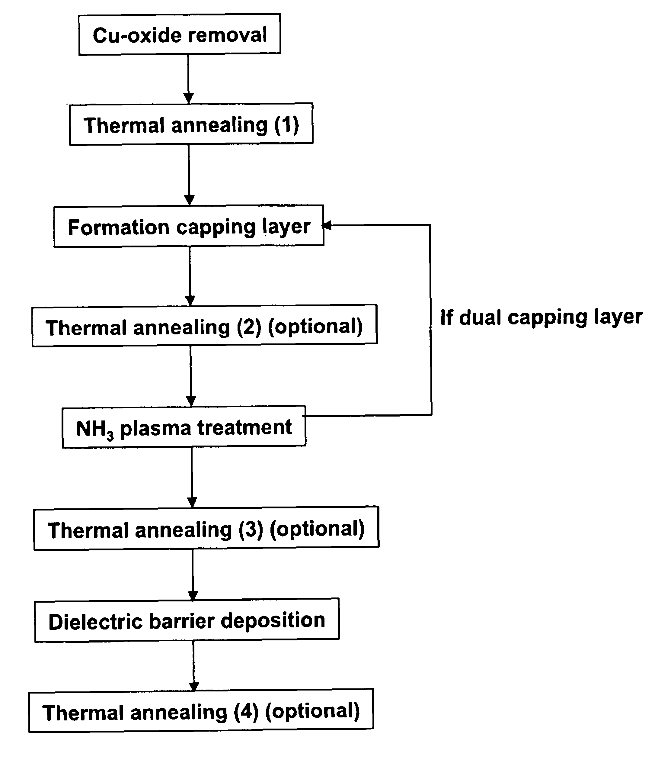
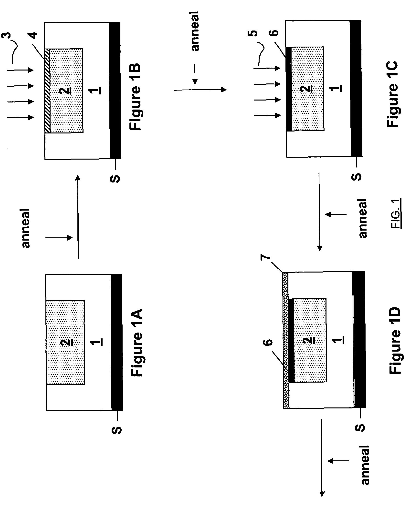
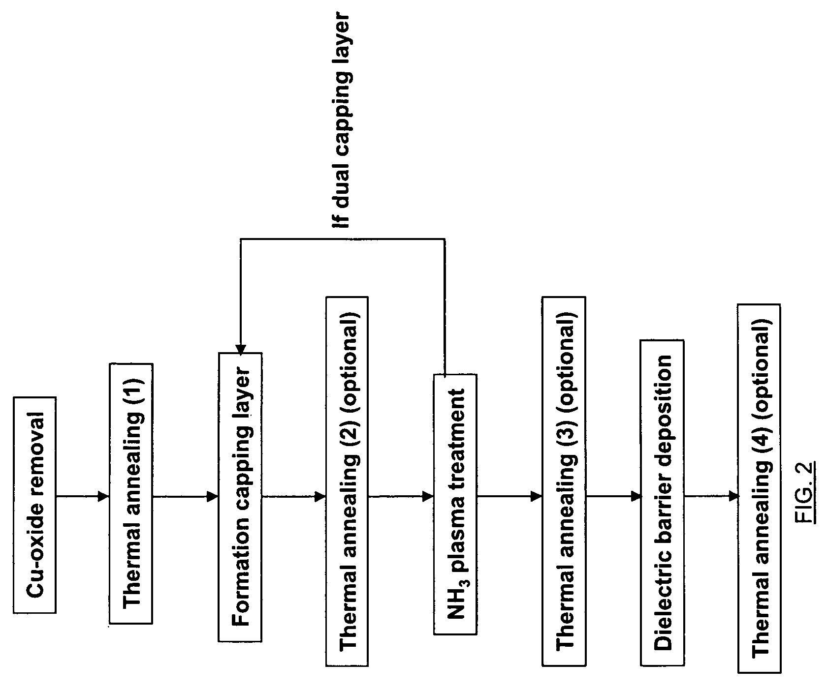
Formation of a CuSixGeyNz Capping Layer

[0178]Suitable process parameters for depositing a CuSixGeyNz capping layer (after having performed a thermal (pre) annealing of the copper structure of e.g. 30 minutes at 400° C.) in a Chemical Vapour Deposition (CVD) chamber are summarized below.

[0179]pressure ˜4 torr

[0180]SiH4 flow ˜100 sccm

[0181]GeH4 flow ˜10 sccm

[0182]N2 flow ˜20000 sccm

[0183]NH3 flow ˜1000 sccm

[0184]Temperature 350° C. for several seconds

[0185]The process parameters for the “in situ” post NH3 plasma treatment are:

[0186]Plasma Power ˜500 W

[0187]NH3 flow ˜1000 sccm

[0188]N2 flow ˜10000 sccm for ˜30 seconds at ˜350 C

[0189]Suitable process parameters for depositing a dual capping layer (stack) CuSixNz / CuGeyNz are similar to the condition mentioned above except the sequential use of GeH4 or SiH4.


PUM

PropertyMeasurementUnit
temperatureaaaaaaaaaa
thicknessaaaaaaaaaa

Abstract

A method is provided for forming a capping layer comprising Cu, N, and also Si and / or Ge onto a copper conductive structure, said method comprising the sequential steps of: forming, at a temperature range between 200° C. up to 400° C., at least one capping layer onto said copper conductive structure by exposing said structure to a GeH4 and / or a SiH4 comprising ambient, performing a NH3 plasma treatment thereby forming an at least partly nitrided capping layer, forming a dielectric barrier layer onto said at least partly nitrided capping layer, wherein prior to said step of forming said at least one capping layer a pre-annealing step of said copper conductive structure is performed at a temperature range between 250° C. up to 450° C.

Description

CROSS-REFERENCE TO RELATED APPLICATIONS[0001]This application claims the benefit under 35 U.S.C. §119(e) of U.S. provisional application Ser. No. 60 / 990,585, filed Nov. 27, 2007, and claims the benefit under 35 U.S.C. §119(a)-(d) of European application No. 08157374.3, filed May 30, 2008, the disclosures of which are hereby expressly incorporated by reference in their entirety and are hereby expressly made a portion of this application.FIELD OF THE INVENTION[0002]Semiconductor processing methods are provided relating to (e.g. copper) damascene advanced interconnect applications for integrated circuit (IC) manufacturing, specifically to the production process of copper interconnect structures in the Back End of Line stages of the production process. A method of depositing a selective capping layer on copper interconnect structures to improve electro-migration (EM) resistance is also provided.BACKGROUND OF THE INVENTION[0003]A commonly used method for forming metal interconnect lines ...

Claims


Application Information

Patent Timeline
Patent Type & Authority Patents(United States)
IPC IPC(8): H01L21/44
CPCH01L21/76846H01L21/76849H01L21/76856H01L21/76867H01L21/76886H01L23/53238H01L2924/0002H01L2924/00
Inventor LIU, CHUNG-SHIYU, CHEN-HUA
Owner TAIWAN SEMICON MFG CO LTD
Why Eureka
Try Eureka