Semiconductor device

a semiconductor device and integrated technology, applied in the field of semiconductor devices, can solve the problems of increasing complexity and/or integration density of semiconductor devices, and achieve the effect of increasing integration density

Active Publication Date: 2015-04-16
SAMSUNG ELECTRONICS CO LTD
View PDF3 Cites 31 Cited by
  • Summary
  • Abstract
  • Description
  • Claims
  • Application Information

AI Technical Summary

Benefits of technology

[0004]Example embodiments of the inventive concept provide a semiconductor device including a first wire of a unidirectional structure and thereby having an increased integration density.

Problems solved by technology

To satisfy these design goals, complexity and / or integration density of semiconductor devices are being increased.

Method used


Image

  • Semiconductor device
  • Semiconductor device
  • Semiconductor device

Examples


Embodiment Construction

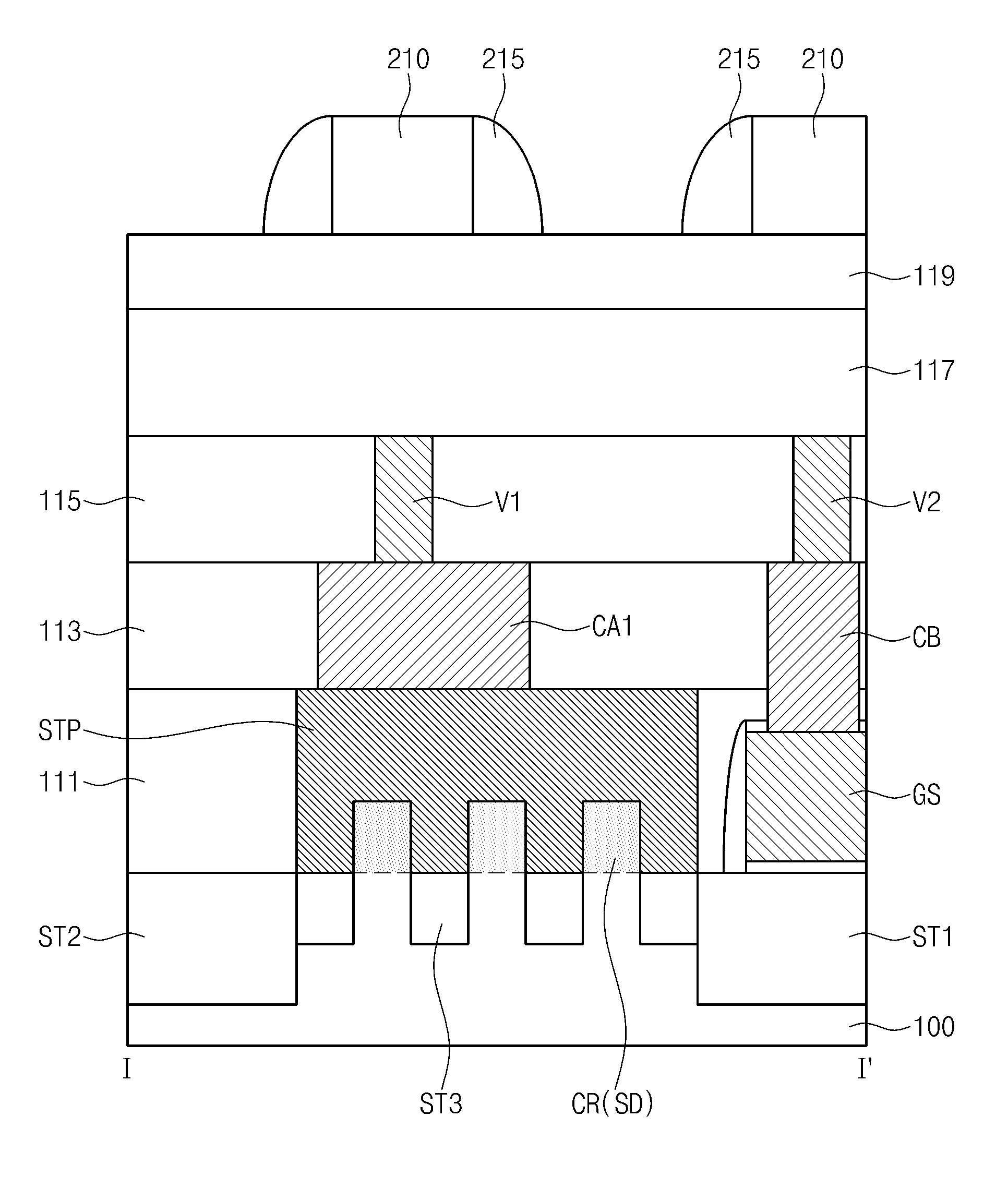
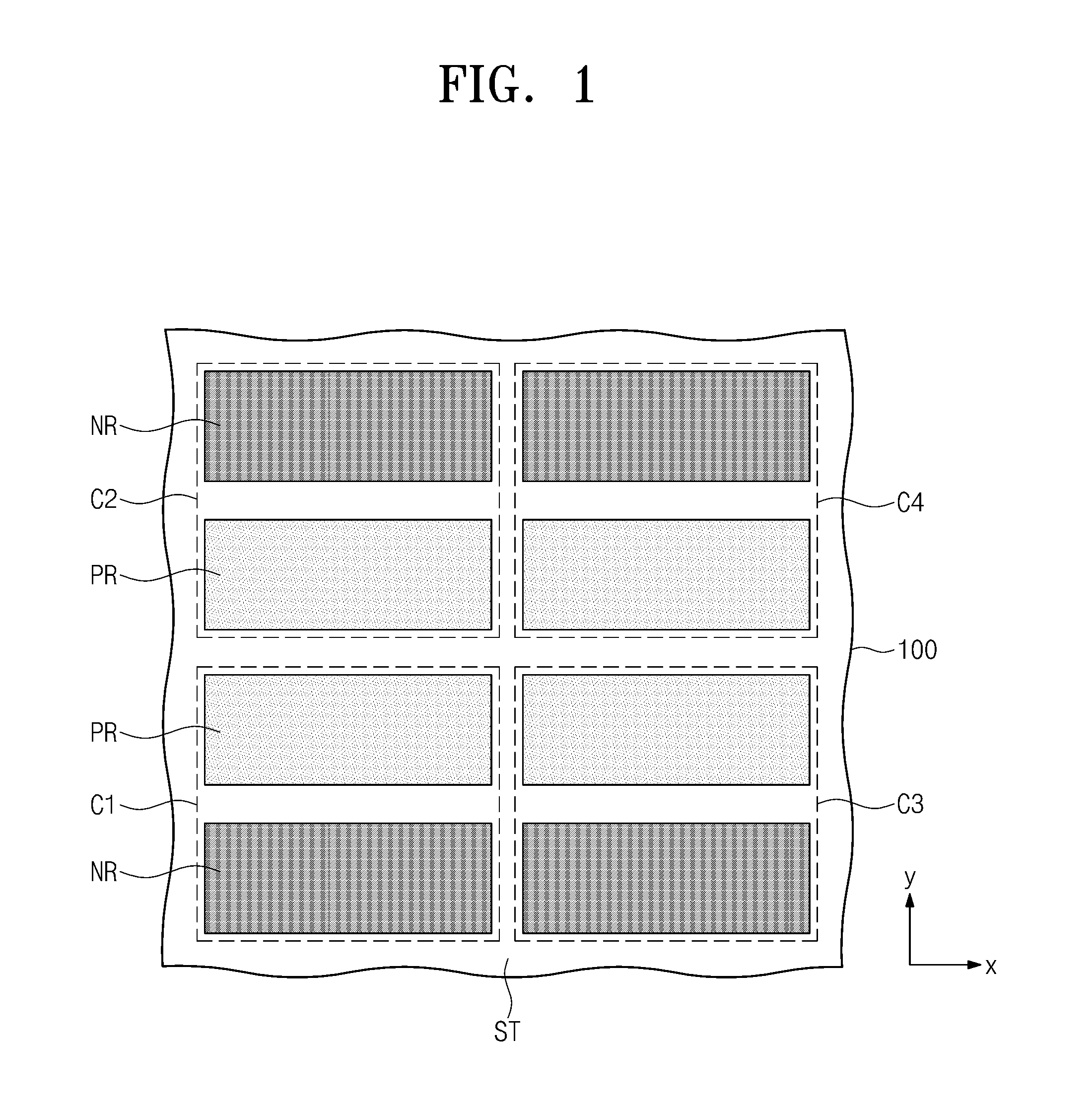
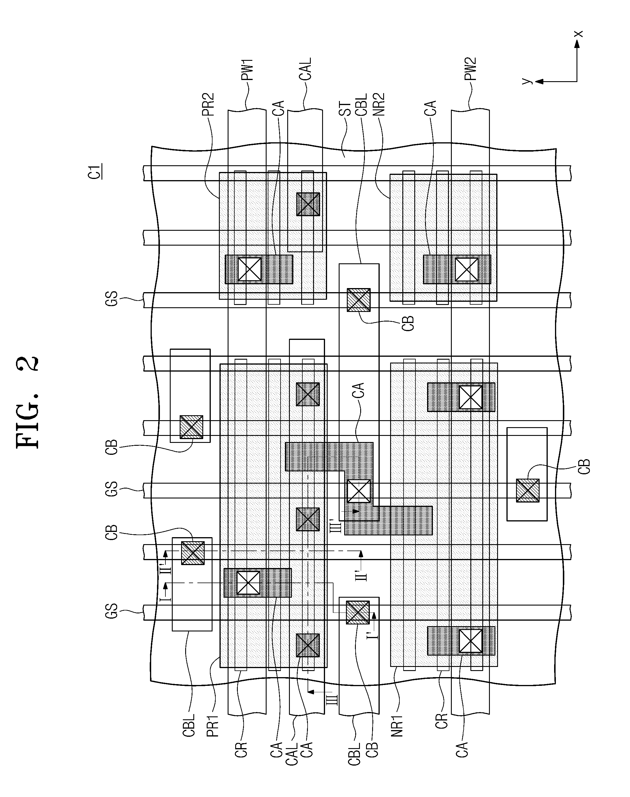
[0056]Example embodiments of the inventive concepts will now be described more fully with reference to the accompanying drawings, in which example embodiments are shown. Example embodiments of the inventive concepts may, however, be embodied in many different forms and should not be construed as being limited to the embodiments set forth herein.

[0057]The terminology used herein is for the purpose of describing particular embodiments only and is not intended to be limiting of example embodiments. As used herein, the singular forms “a,”“an” and “the” are intended to include the plural forms as well, unless the context clearly indicates otherwise. As used herein the term “and / or” includes any and all combinations of one or more of the associated listed items. It will be further understood that the terms “comprises”, “comprising”, “includes” and / or “including,” if used herein, specify the presence of stated features, integers, steps, operations, elements and / or components, but do not pr...


PUM


Abstract

Provided is a semiconductor device including a substrate with a plurality of logic cells, transistors provided in the plurality of logic cells, contact plugs connected to electrodes of the transistors, first via plugs in contact with top surfaces of the contact plugs, and first wires in contact with top surfaces of the first via plugs. The first wires may include a common conductive line connected to the plurality of logic cells through the contact plugs, and all of the first wires may be shaped like a straight line extending parallel to a specific direction.

Description

CROSS-REFERENCE TO RELATED APPLICATIONS[0001]This U.S. non-provisional patent application claims priority under 35 U.S.C. §119 to Korean Patent Application No. 10-2013-0121012, filed on Oct. 11, 2013, in the Korean Intellectual Property Office, the entire contents of which are hereby incorporated by reference.BACKGROUND OF THE INVENTION[0002]Example embodiments of the inventive concept relate to a semiconductor device, and in particular, to a semiconductor device with a plurality of logic cells.[0003]Semiconductor devices are increasingly being used in consumer, commercial and other electronic devices. The semiconductor devices may be classified into a memory device for storing data, a logic device for processing data, and a hybrid device including both of memory and logic elements. Due to the increased demand for electronic devices with fast speed and / or low power consumption, the semiconductor devices are designed to provide high reliability, high performance, and / or multiple func...

Claims


Application Information

Patent Timeline
Patent Type & Authority Applications(United States)
IPC IPC(8): H01L27/24H01L23/538
CPCH01L27/2454H01L23/5384H01L27/0207H01L27/11807H01L2924/0002H03K19/1736H01L2924/00H01L21/28H01L21/3205H01L23/535H01L29/0649
Inventor AZMAT, RAHEELSENGUPTA, RWIKPARK, CHULHONGCHUN, KWANYOUNG
Owner SAMSUNG ELECTRONICS CO LTD
Why Eureka
Try Eureka