Liquid crystal display including nanocapsule layer

a liquid crystal display and nano-capsule technology, applied in the field of liquid crystal display devices, can solve the problems of reduced display quality, reduced production efficiency, and disadvantages of lcd brightness compared with other types of flat display displays, and achieve the effect of improving response speed and/or production efficiency

Inactive Publication Date: 2015-04-23
LG DISPLAY CO LTD
View PDF3 Cites 37 Cited by
  • Summary
  • Abstract
  • Description
  • Claims
  • Application Information

AI Technical Summary

Benefits of technology

[0026]An advantage of the present invention is to provide an LCD including a nanocapsule layer that can improve its response speed and / or production efficiency.
[0027]Additional features and advantages of the invention will be set forth in the description which follows, and in part will be apparent from the description, or may be learned by practice of the invention. These and other advantages of the invention will be realized and attained by the structure particularly pointed out in the written description and claims hereof as well as the appended drawings.
[0028]To achieve these and other advantages and in accordance with the purpose of the present invention, as embodied and broadly described herein, a liquid crystal display device may include a first substrate; a first electrode on the first substrate, the first electrode including a plurality of first inclined planes; a nanocapsule liquid crystal layer on the first electrode, the nanocapsule liquid crystal layer including a plurality of nano-sized capsules dispersed in a buffer layer, each of the plurality of nano-sized capsules including nematic liquid crystal molecules having a negative dielectric constant anisotropy; and a second electrode on the nanocapsule liquid crystal layer, the second electrode including a plurality of second inclined planes facing the plurality of first inclined planes, wherein the nanocapsule liquid crystal layer is substantially, optically isotropic in a normal state, and is optically anisotropic when a voltage is applied to the first and second electrodes.
[0029]In another aspect, a liquid crystal display device may include a first substrate; a first polarizing plate on an outer surface of the first substrate; a first electrode on an inner surface of the first substrate; a nanocapsule liquid crystal layer that is on the first electrode and includes nano-sized capsules which are each filled with nematic liquid crystal molecules of negative dielectric constant anisotropy and are dispersed in a buffer layer; and a second electrode on the nanocapsule liquid crystal layer; a phase retardation film that is on the second electrode and has a phase retardation value of λ / 4; and a second polarizing plate on the phase retardation film, wherein the nanocapsule liquid crystal layer has an optical anisotropy according to a voltage difference between voltages applied to the first and second electrodes, and has an optical isotropy when no voltages are applied to the first and second electrodes.
[0030]In another aspect, a liquid crystal display device may include a first substrate; a plurality of first electrodes on an inner surface of the first substrate; a nanocapsule liquid crystal layer that is on the plurality of first electrodes and includes nano-sized capsules which are each filled with nematic liquid crystal molecules of negative dielectric constant anisotropy and are dispersed in a buffer layer; and a second electrode on the nanocapsule liquid crystal layer, wherein the nanocapsule liquid crystal layer has an optical anisotropy according to a voltage difference between voltages applied to the first and second electrodes, and has an optical isotropy when no voltages are applied to the first and second electrodes.
[0031]In another aspect, a reflective type liquid crystal display device may include a liquid crystal panel that includes a first electrode, a second electrode, and a nanocapsule liquid crystal layer between the first and second electrodes; a polarizing plate that is on a surface of the liquid crystal layer through which an external light enters; a phase retardation plate between the polarizing plate and the liquid crystal panel; and a reflection plate that reflects light passing through the nanocapsule liquid crystal layer, wherein the nanocapsule liquid crystal layer has an optical anisotropy according to a voltage difference between voltages applied to the first and second electrodes, and has an optical isotropy when no voltages are applied to the first and second electrodes.

Problems solved by technology

As such, the LCD has disadvantage in brightness compared with other types of flat display displays.
Moreover, the LCD has slow response speed, and thus display quality is reduced due to afterimage.
Moreover, the LCD requires many production processes, and thus production efficiency is reduced.
However, in the reflective type LCD, light leakage is easily caused by an external force, and thus display quality is reduced.
Moreover, the reflective type LCD also requires many production processes, and thus production efficiency is reduced.

Method used


Image

  • Liquid crystal display including nanocapsule layer
  • Liquid crystal display including nanocapsule layer
  • Liquid crystal display including nanocapsule layer

Examples


first embodiment

[0101]FIGS. 5A and 5B are schematic views illustrating an LCD according to the first embodiment of the present invention.

[0102]Referring to FIGS. 5A and 5B, the LCD of the first embodiment includes the liquid crystal panel 110 and the backlight unit 160.

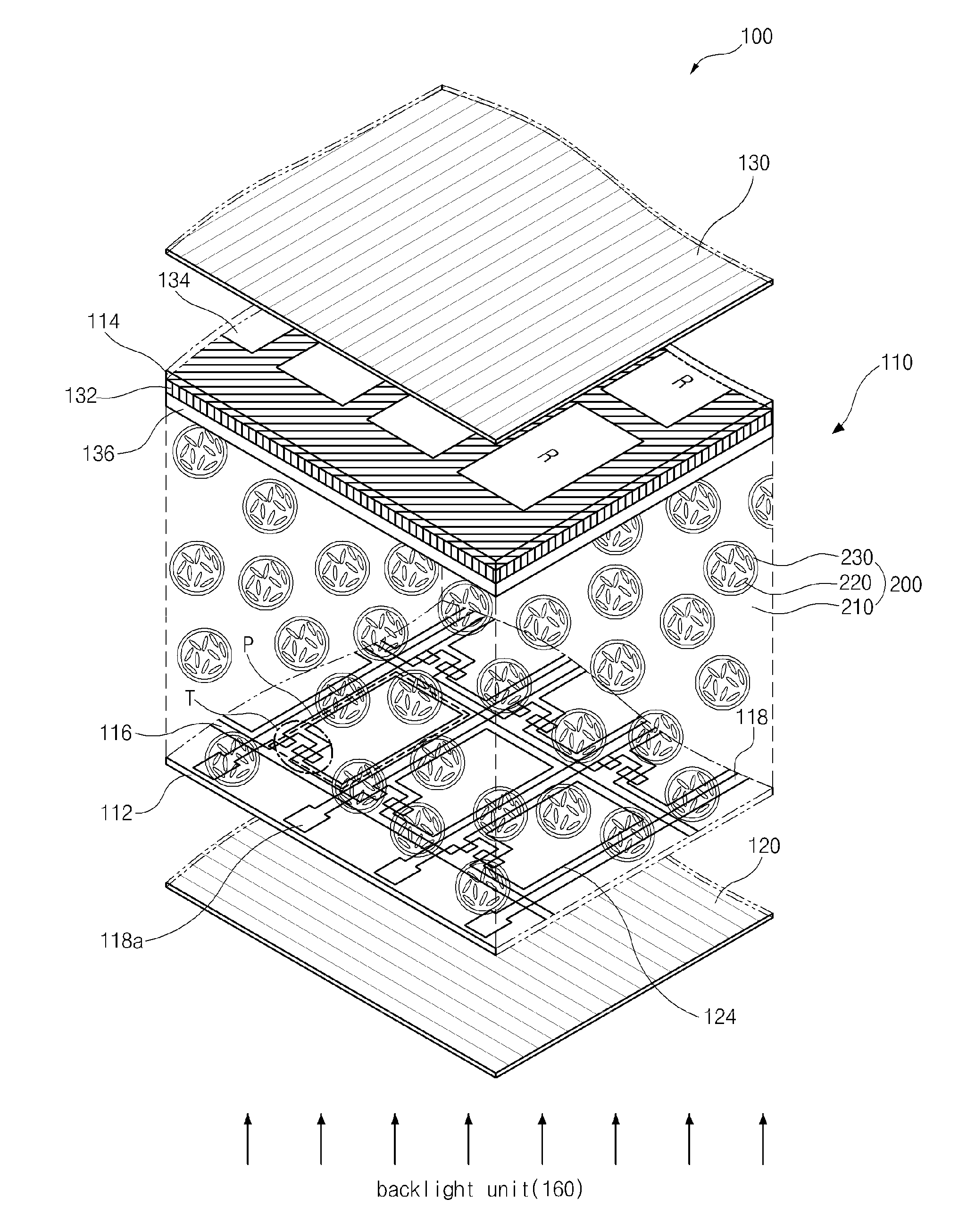
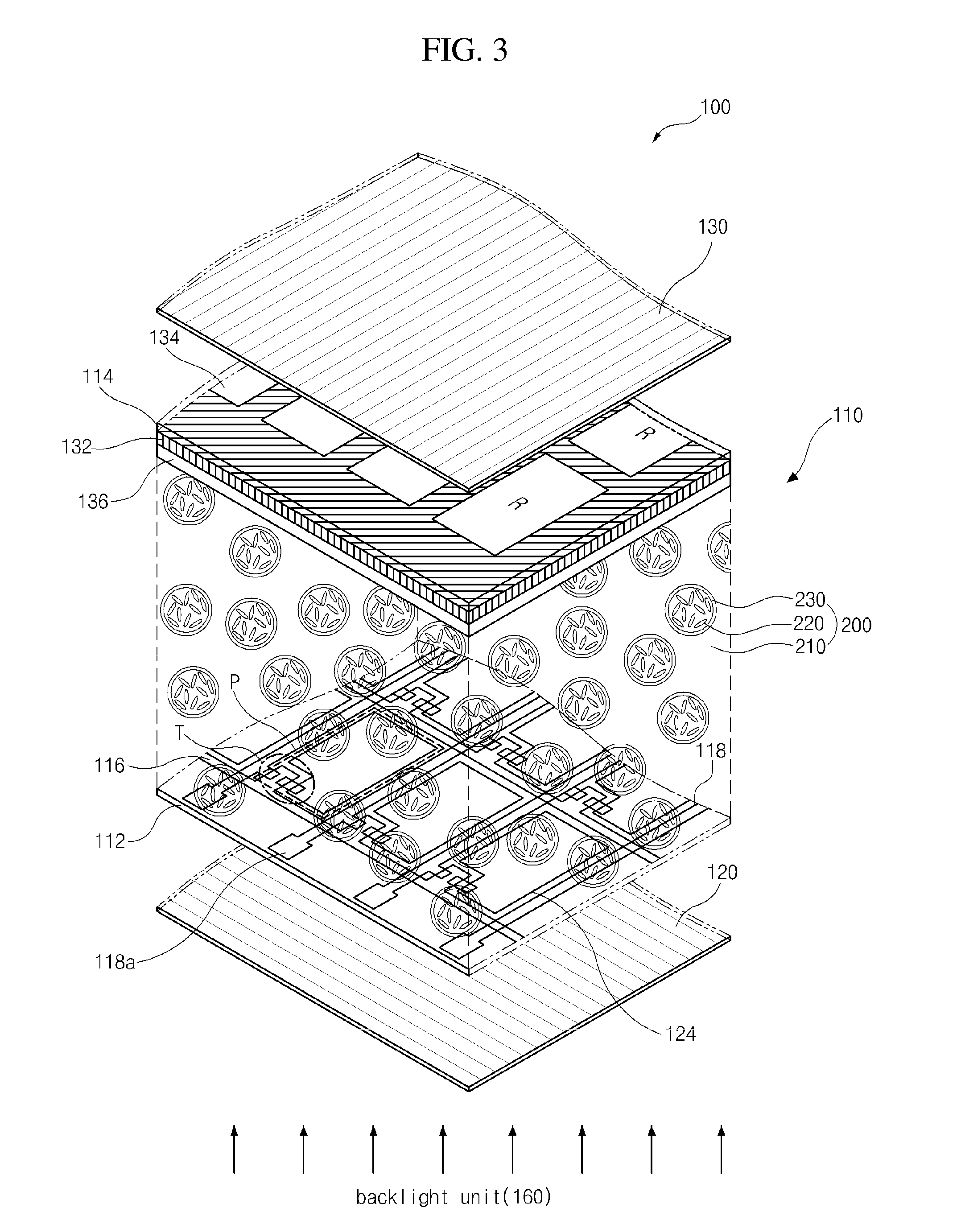
[0103]The liquid crystal panel 110 includes the first and second substrates 112 and 114 facing each other, the nanocapsule liquid crystal layer 200, and the first and second polarizing plates 120 and 130 on the outer surfaces of the first and second substrates 112 and 114, respectively.

[0104]The liquid crystal panel 110 may be a vertical alignment (VA) mode liquid crystal panel. The thin film transistor (T of FIG. 3) and the pixel electrode 124 are formed on the inner surface of the first substrate 112. The black matrix (132 of FIG. 3), the color filters 134, and the common electrode 136 are formed on the inner surface of the second substrate 114. An overcoat layer may be formed covering the black matrix 132 and the color filters 134...

second embodiment

[0142]FIGS. 8A and 8B are schematic views illustrating an LCD according to a second embodiment of the present invention. Explanations of parts similar to parts of the above first embodiment may be omitted.

[0143]Referring to FIGS. 8A and 8B, the LCD (100 of FIG. 3) of the second embodiment includes the liquid crystal panel 110 and the backlight unit 160.

[0144]The liquid crystal panel 110 includes the first and second substrates 112 and 114 facing each other, the nanocapsule liquid crystal layer 200, and the first and second polarizing plates 120 and 130 on the outer surfaces of the first and second substrates 112 and 114, respectively.

[0145]The liquid crystal panel 110 may be a vertical alignment (VA) mode liquid crystal panel. The thin film transistor (T of FIG. 3) and the pixel electrode 124 are formed on the inner surface of the first substrate 112. The black matrix (132 of FIG. 3), the color filters 134, and the common electrode 136 are formed on the inner surface of the second s...

third embodiment

[0168]FIG. 11A is a schematic view illustrating an LCD according to a third embodiment of the present invention. Explanations of parts similar to parts of the above first and second embodiments may be omitted.

[0169]Referring to FIG. 11A, the LCD (100 of FIG. 3) of the third embodiment includes the liquid crystal panel 110 and the backlight unit 160.

[0170]The liquid crystal panel 110 includes the first and second substrates 112 and 114 facing each other, the nanocapsule liquid crystal layer 200, and the first and second polarizing plates 120 and 130 on the outer surfaces of the first and second substrates 112 and 114, respectively.

[0171]The liquid crystal panel 110 may be a vertical alignment (VA) mode liquid crystal panel. The thin film transistor (T of FIG. 3) and the pixel electrode 124 are formed on the inner surface of the first substrate 112. The black matrix (132 of FIG. 3), the color filters 134, and the common electrode 136 are formed on the inner surface of the second subst...


PUM

PropertyMeasurementUnit
diameteraaaaaaaaaa
thicknessaaaaaaaaaa
diameteraaaaaaaaaa

Abstract

Disclosed is a liquid crystal display device that may include a first substrate; a first electrode on the first substrate, the first electrode including a plurality of first inclined planes; a nanocapsule liquid crystal layer on the first electrode, the nanocapsule liquid crystal layer including a plurality of nano-sized capsules dispersed in a buffer layer, each of the plurality of nano-sized capsules including nematic liquid crystal molecules having a negative dielectric constant anisotropy; and a second electrode on the nanocapsule liquid crystal layer, the second electrode including a plurality of second inclined planes facing the plurality of first inclined planes, wherein the nanocapsule liquid crystal layer is substantially, optically isotropic in a normal state, and is optically anisotropic when a voltage is applied to the first and second electrodes.

Description

[0001]This application claims the benefit of Korean Patent Application Nos. 10-2013-01126534, 10-2013-0151308 and 10-2013-0152890, filed on Oct. 23, 2013, Dec. 6, 2013 and Dec. 10, 2013, respectively, which are hereby incorporated by reference for all purposes as if fully set forth herein.BACKGROUND OF THE INVENTION[0002]1. Field of the Invention[0003]The present invention relates to a liquid crystal display device (LCD), and more particularly, to an LCD including a nanocapsule layer and method for manufacturing the same.[0004]2. Discussion of the Prior Art[0005]Recently, facing information society, display field of displaying electric information signals has been rapidly advanced, and flat display devices having high performances of thin profile, lightweight and low power consumption have been developed and used. Among these flat display devices, liquid crystal display devices (LCDs) are widely used.[0006]FIG. 1 is a cross-sectional view illustrating an LCD according to the prior a...

Claims


Application Information

Patent Timeline
Patent Type & Authority Applications(United States)
IPC IPC(8): G02F1/1334G02F1/137G02F1/1333G02F1/1335G02F1/1368
CPCG02F1/1334G02F1/133603G02F1/133553G02F1/133528G02F1/1368G02F2001/133541G02F1/13718G02F1/133514G02F1/13338G02F1/133524G02F1/133305G02F1/134309G02F1/133541G02B6/0056G02F1/133707G02F2202/36G02F1/13712G02F1/13363G02F2203/02G02F1/133531G02F1/133638
Inventor KIM, KYEONG-JINHWANG, JUNG-IMJEON, JI-NAHA, KYUNG-SUCHOI, MIN-GEUN
Owner LG DISPLAY CO LTD
Why Eureka
Try Eureka