Wirebond recess for stacked die

Active Publication Date: 2015-04-30
NXP USA INC
View PDF11 Cites 3 Cited by
  • Summary
  • Abstract
  • Description
  • Claims
  • Application Information

AI Technical Summary

Benefits of technology

The present invention provides a solution for stacking multiple semiconductor device die in a semiconductor device package while minimizing the thickness of the package. By incorporating notch structures on the semiconductor device die, the dimensions of the package can be reduced while still allowing for wire bond connections between the die. The use of notch structures also allows for a reduction in the thickness of the semiconductor device package. The invention also addresses the challenge of stacking semiconductor device die while maintaining functionality and minimizing package substrate area.

Problems solved by technology

One challenge is that each semiconductor device die must retain functionality, while reducing dimensionality.
In order to provide sufficient space for wire bonds to be formed and routed, die spacers are often utilized, which increases thickness of the stack, or smaller die are stacked on the top of the stack, which reduces options in how a stack is formed and can cause issues with stacks formed of equal sized die.

Method used


Image

  • Wirebond recess for stacked die
  • Wirebond recess for stacked die
  • Wirebond recess for stacked die

Examples


Embodiment Construction

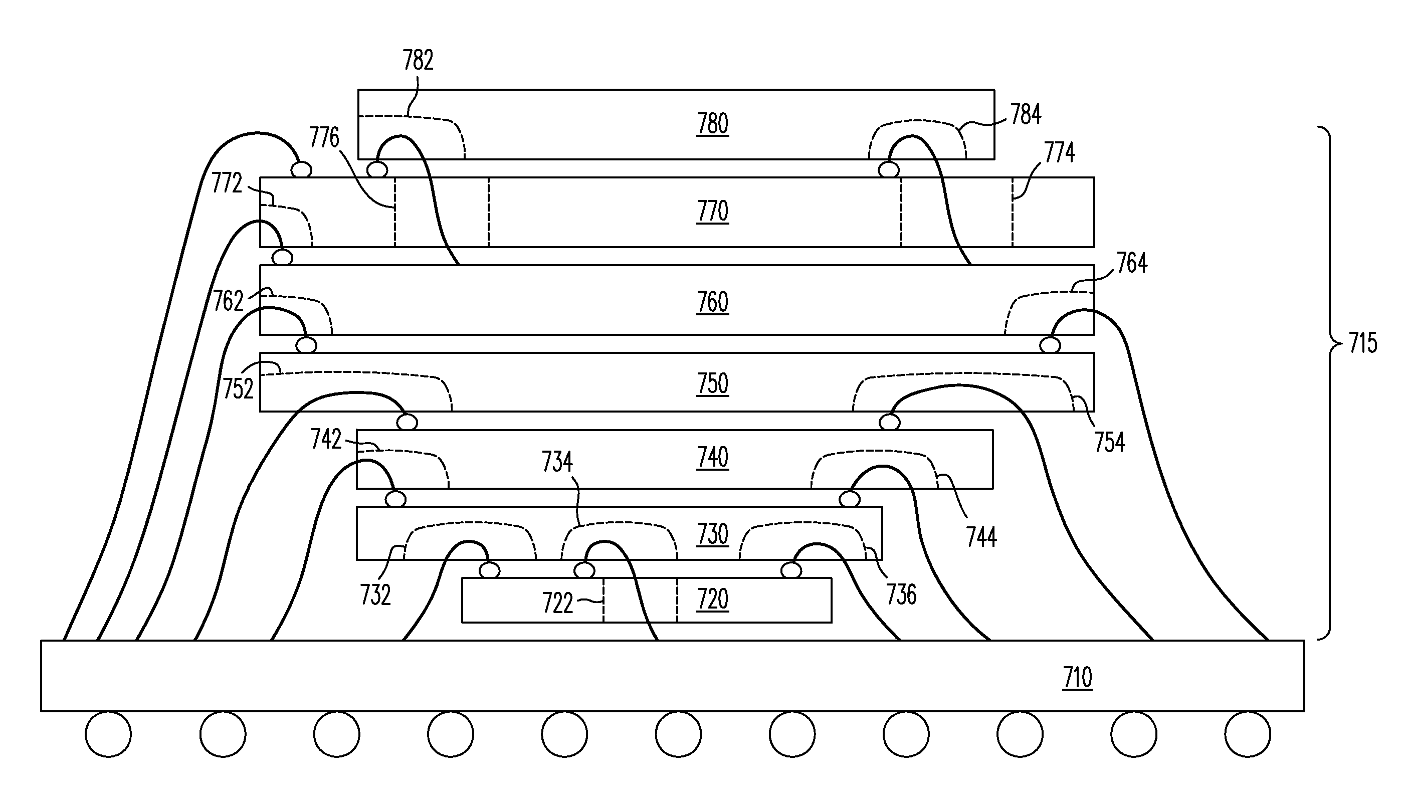
[0016]Embodiments of the present invention provide for a first semiconductor device die having a bottom edge incorporating a notch structure that allows sufficient height and width clearance for a wire bond connected to a bond pad on an active surface of a second semiconductor device die upon which the first semiconductor device die is stacked. Use of such notch structures reduces a height of a stack incorporating the first and second semiconductor device die, thereby also reducing a thickness of a semiconductor device package incorporating the stack.

[0017]In order to provide multiple functionalities in a semiconductor device package, multiple semiconductor device die can be incorporated in the package. In order to provide the desired functionalities in a package consuming as little floor plan area as possible, the multiple semiconductor device die can be stacked one on top of the other. While decreasing the floor plan area of the semiconductor device package, such a stacked configu...


PUM


Abstract

A first semiconductor device die is provided having a bottom edge incorporating a notch structure that allows sufficient height and width clearance for a wire bond connected to a bond pad on an active surface of a second semiconductor device die upon which the first semiconductor device die is stacked. Use of such notch structures reduces a height of a stack incorporating the first and second semiconductor device die, thereby also reducing a thickness of a semiconductor device package incorporating the stack.

Description

BACKGROUND[0001]1. Field[0002]This disclosure relates generally to semiconductor device packaging, and more specifically, to stacking multiple semiconductor device die while minimizing stack thickness.[0003]2. Related Art[0004]Semiconductor device packaging often involves incorporating multiple semiconductor device die having a variety of functionalities in an encapsulant, so that multi-functional packages can be provided as a unit. As demands for greater functionality in smaller and smaller devices increases, a goal of semiconductor device packaging is to incorporate the desired number of semiconductor device die in as dimensionally small a package as possible. Package thickness can be reduced by reducing thicknesses of various semiconductor device die stacked in the package, which can thereby reduce encapsulant thickness. One challenge is that each semiconductor device die must retain functionality, while reducing dimensionality.[0005]In addition, electrical contacts on the variou...

Claims


Application Information

Patent Timeline
IPC IPC(8): H01L23/00H01L25/065
CPCH01L24/02H01L24/80H01L2224/80001H01L2224/04H01L25/0657H01L2224/32145H01L2224/32225H01L2224/48091H01L2224/48465H01L2224/73265H01L2924/10158H01L2924/15311H01L24/29H01L24/32H01L2224/04042H01L2224/2919H01L2224/48145H01L2224/48227H01L2225/0651H01L2225/06506H01L2224/92165H01L24/83H01L24/85H01L24/92H01L29/0657H01L2924/10156H01L24/45H01L2224/45124H01L2224/45144H01L2224/45147H01L24/48H01L2924/12042H01L24/73H01L2924/00014H01L2924/00012H01L2924/00H01L2224/85399H01L2224/05599
Inventor PHAM, TIM V.MCSHANE, MICHAEL B.PELLEY, PERRY H.STEPHENS, TAB A.
Owner NXP USA INC
Why Eureka
Try Eureka