Glass substrate for electronic amplification and method for manufacturing the same

Inactive Publication Date: 2015-04-30
HOYA CORP
View PDF26 Cites 10 Cited by
  • Summary
  • Abstract
  • Description
  • Claims
  • Application Information

AI Technical Summary

Benefits of technology

[0023]According to the present invention, even in a case of using the glass substrate as the base material of the substrate

Problems solved by technology

However, in the GEM having the abovementioned structure, the film member made of polyimide, etc., is used as a base material of the substrate for e

Method used


Image

  • Glass substrate for electronic amplification and method for manufacturing the same
  • Glass substrate for electronic amplification and method for manufacturing the same
  • Glass substrate for electronic amplification and method for manufacturing the same

Examples


example 1

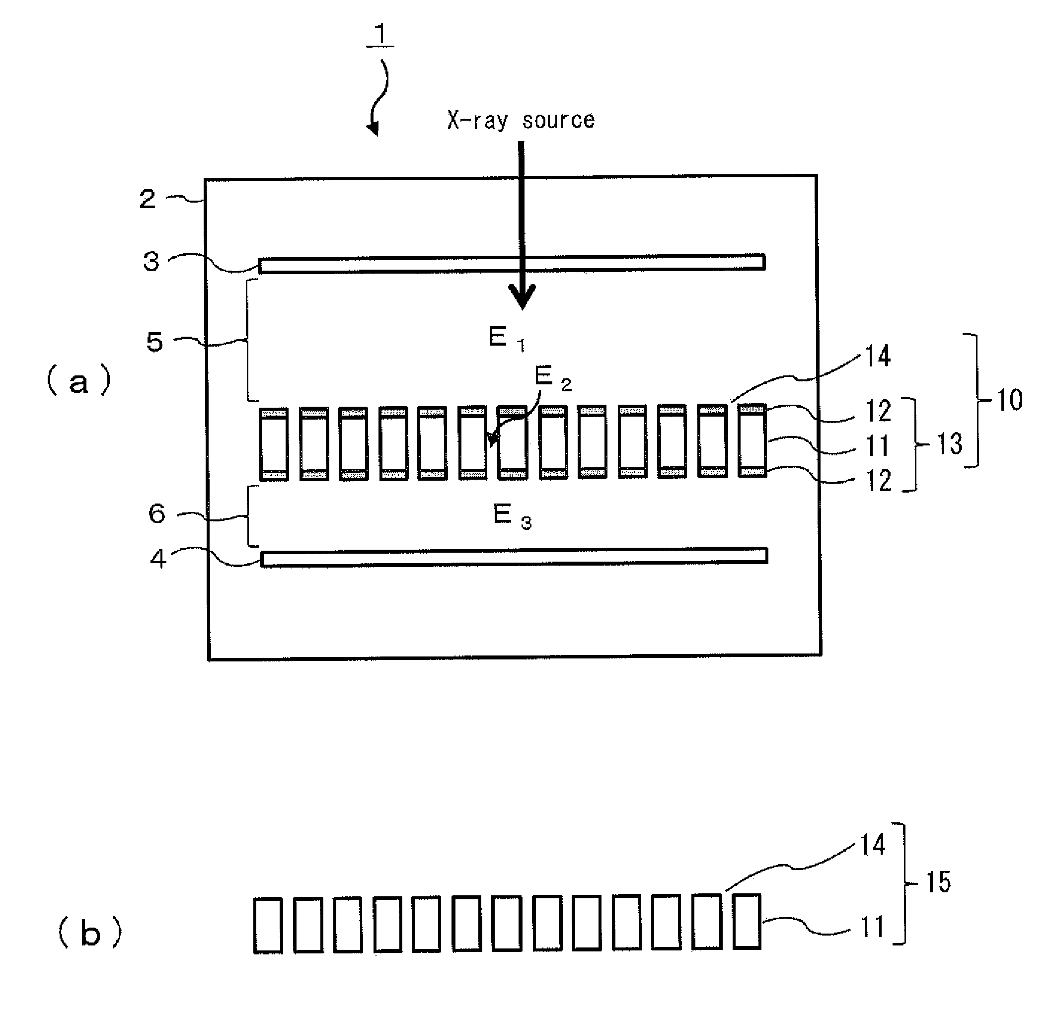
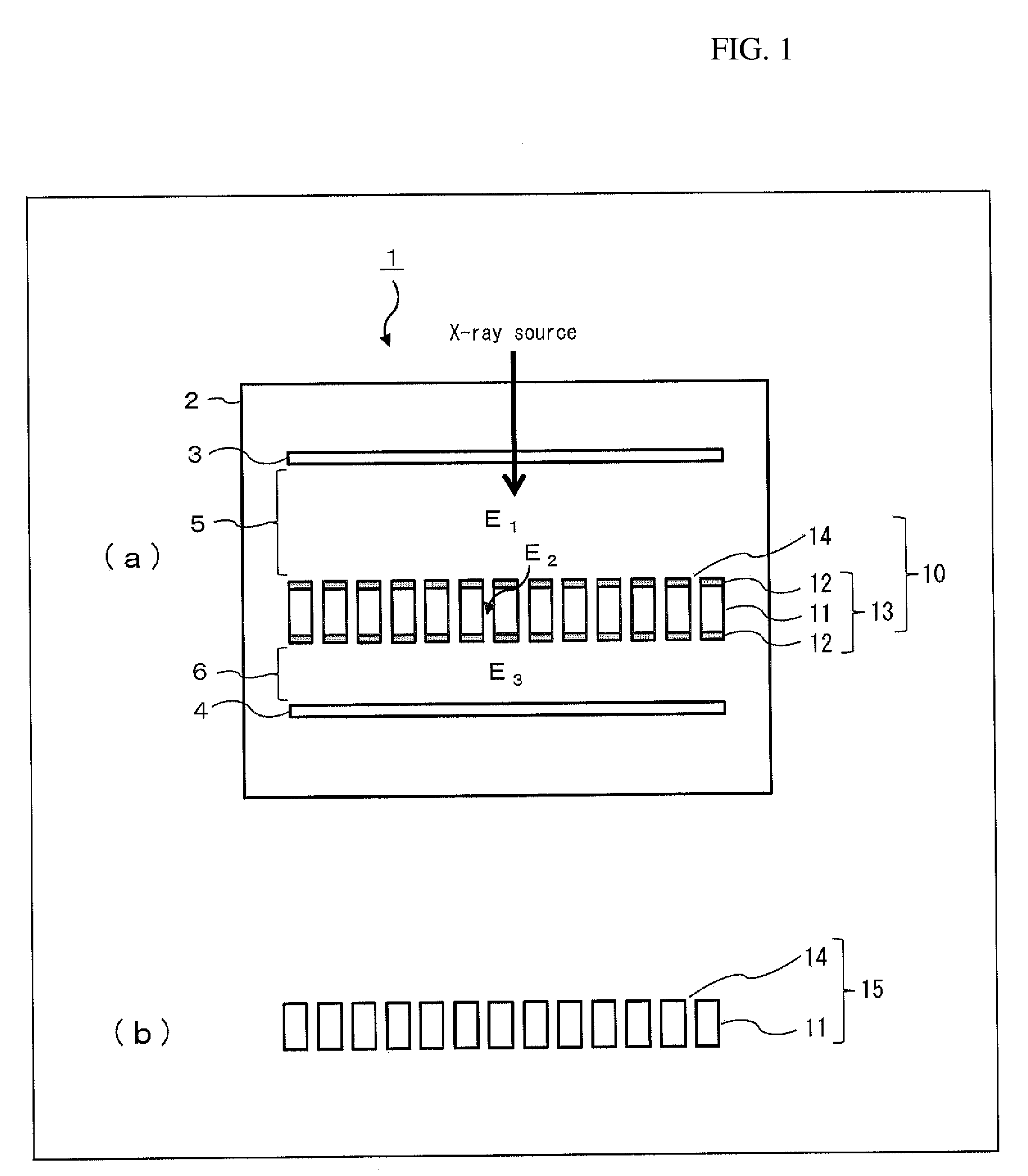
[0099]In example 1, the glass substrate 15 for electronic amplification was constituted, having the through holes 14 formed on the plate-like member 11 of a plate thickness of 700 μm and made of “PEG3”, the through holes having a hole diameter of 140 μm and arranged at a pitch of 280 μm. As for the glass substrate 15 for electronic amplification having such a structure, the insulation resistance in the plate thickness direction per plane of 100 cm2 was measured, and it was found that the glass substrate 15 had the insulation resistance of 410 MΩ when voltage of 1000V was applied thereto.

[0100]Then, the substrate 10 for electronic amplification constituted using the glass substrate 15 for electronic amplification, was disposed in the chamber 2 of the detector 1. The chamber 2 is configured so that X-ray of 6 keV is incident therein, the X-ray being collimated by 100 μmφ from an outside radiation source.

[0101]Under such a circumstance, potential difference of about 1800 V was applied ...

example 2

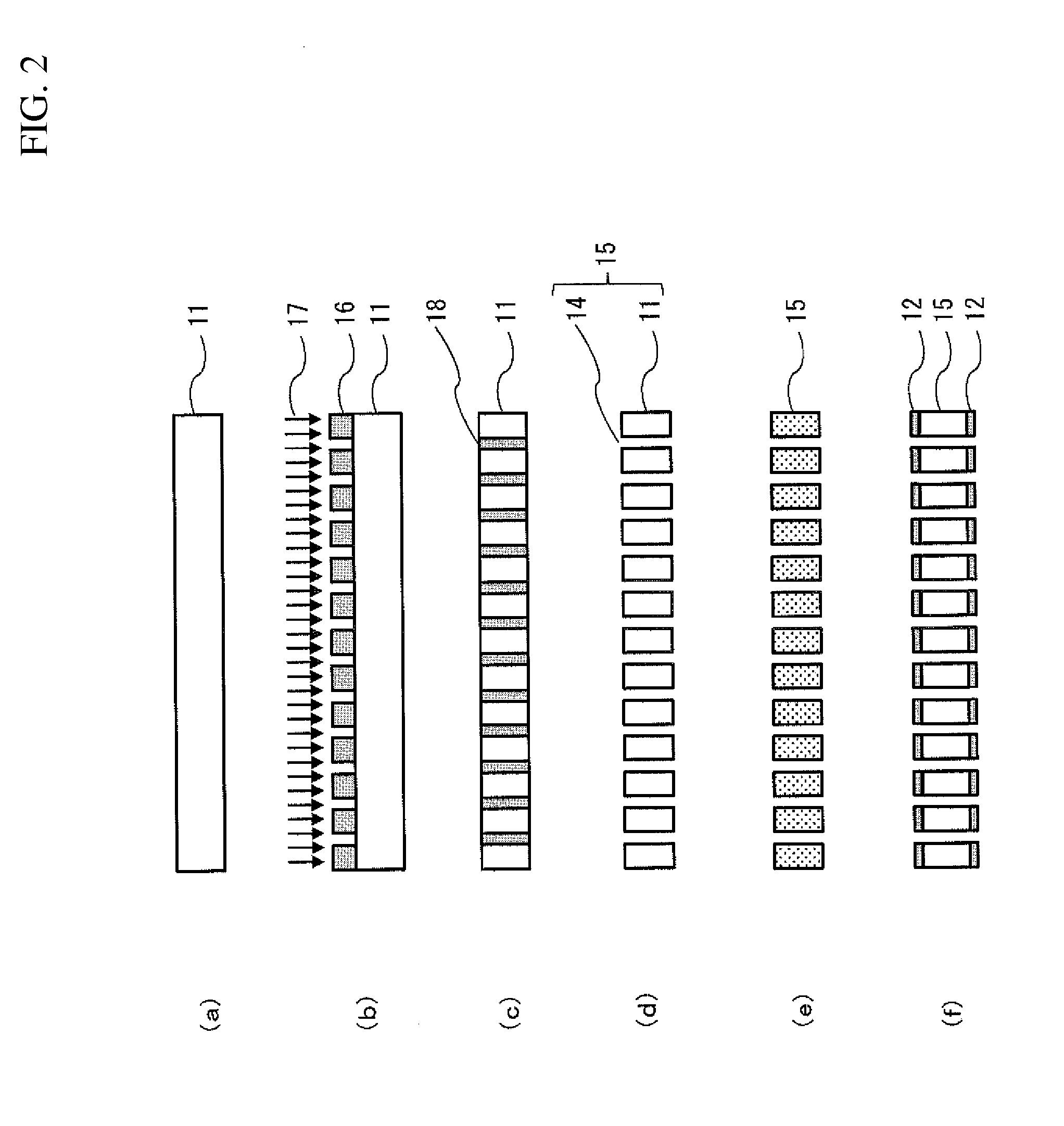
[0102]In example 2, the glass substrate 15 for electronic amplification made of “PEG3C” was constituted, having the through holes 14 formed on the plate-like member 11 of a plate thickness of 840 μm and made of “PEG3C”, the through holes having a hole diameter of 140 μm and arranged at a pitch of 280 μm. Then, etching treatment was applied to the glass substrate 15 for electronic amplification by an etching solution in which NH4F / HF and (NH4)2SO4 were mixed for 35 minutes, to thereby roughen the inner wall surface of the through hole 14. As for the glass substrate 15 for electronic amplification having such a structure, the insulation resistance in the plate thickness direction per plane of 100 cm2 was measured, and it was found that the glass substrate 15 had the insulation resistance of 450 MΩ when voltage of 1000V was applied thereto.

[0103]Then, the substrate 10 for electronic amplification constituted using the glass substrate 15 for electronic amplification having the abovement...


PUM

PropertyMeasurementUnit
Electrical resistanceaaaaaaaaaa
Areaaaaaaaaaaa
Thicknessaaaaaaaaaa

Abstract

There is provided a glass substrate for electronic amplification having through holes formed on a plate-like glass member and used for causing an electron avalanche in the through holes, wherein a shape of the glass substrate for electronic amplification and a material of the glass member are determined so that an insulation resistance in a plate thickness direction per plane of 100 cm2 is 107 to 1011Ω.

Description

FIELD OF THE INVENTION [0001]The present invention relates to a glass substrate for electronic amplification and a method for manufacturing the same.DESCRIPTION OF RELATED ART [0002]In recent years, a detector for detecting particle beams or electromagnetic waves utilizing electron avalanche amplification by a gas electron multiplier (abbreviated as “GEM” hereafter), is known.[0003]A general GEM has a plurality of through holes formed on a plate-like film member made of polyimide, etc., so as to pass through its front and rear surfaces, and has a substrate for electronic amplification with both surfaces of its film member coated with copper. Then, potential difference is applied between two electrodes using a copper thin film coating both surfaces of the film member in a state that the substrate for electronic amplification is disposed in a detection gas. Then a strong electric field is created in the plurality of through holes, and an electron avalanche amplification is caused by t...

Claims


Application Information

Patent Timeline
IPC IPC(8): C03C15/00G01R31/12H01J47/00H01J43/04
CPCC03C15/00H01J47/001G01R31/1227H01J43/04G01T1/2935Y10T428/24273H01J47/02H01J43/246
Inventor FUSHIE, TAKASHIKIKUCHI, HAJIME
Owner HOYA CORP
Why Eureka
Try Eureka