Check patentability & draft patents in minutes with Patsnap Eureka AI!

Determining Information for Defects on Wafers

a technology for determining information and defects, applied in the direction of fluorescence/phosphorescence, luminescent dosimeters, optical radiation measurement, etc., can solve the problems of increasing the difficulty of detecting defects on the wafer, noise in the output of tools, and not having much flexibility in the wavelengths of light used for excitation and emission

Active Publication Date: 2015-05-07
KLA CORP
View PDF9 Cites 5 Cited by
  • Summary
  • Abstract
  • Description
  • Claims
  • Application Information

AI Technical Summary

Benefits of technology

The patent text describes a system and method for detecting and analyzing defects on a wafer. The system includes an illumination system that directs light to the wafer, a detection system that only detects the light emitted by the wafer, and a computer system that analyzes the detected light to determine information about the defects on the wafer. The system is designed to cause fluorescence from certain materials on the wafer without causing fluorescence from other materials. The method can include various steps and can be performed using different systems. Overall, the invention allows for improved accuracy and efficiency in identifying and analyzing defects on wafers.

Problems solved by technology

However, as the dimensions of semiconductor devices decrease, inspection becomes even more important to the successful manufacture of acceptable semiconductor devices because smaller defects can cause the devices to fail.
However, such tools generally do not have much flexibility in the wavelengths of light used for excitation and the wavelengths of emission that are detected by the tools.
In addition, many such tools are not configured for inspection of patterned wafers containing rectilinear or other patterns that scatter light strongly or can otherwise cause noise in the output of the tools that increases the difficulty of detecting defects on the wafers.

Method used


Image

  • Determining Information for Defects on Wafers
  • Determining Information for Defects on Wafers
  • Determining Information for Defects on Wafers

Examples


Embodiment Construction

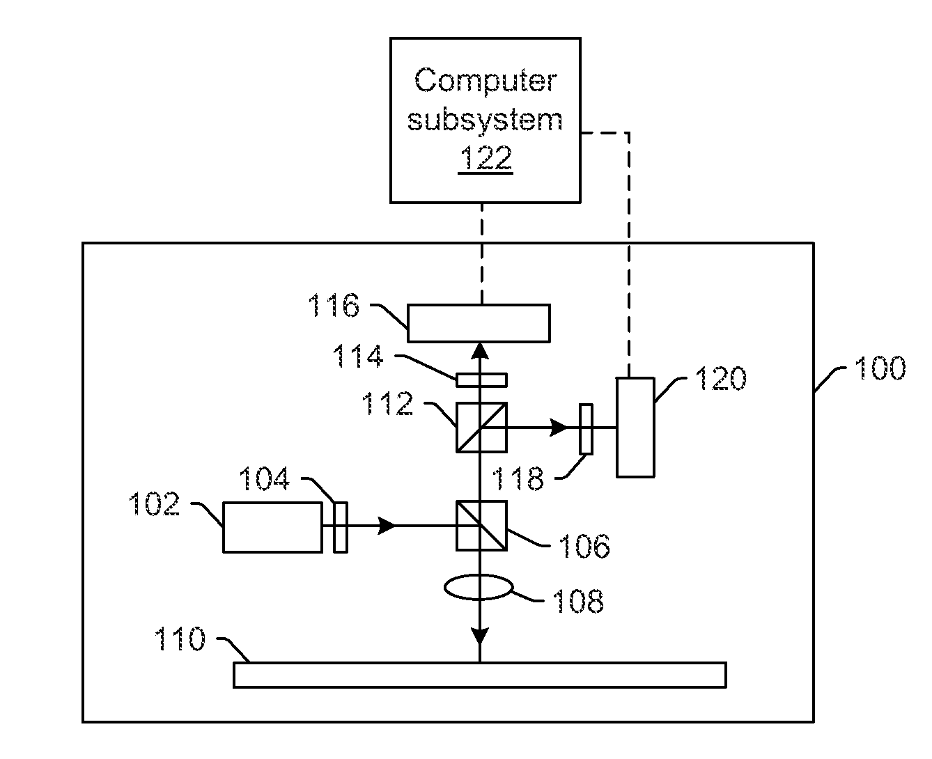
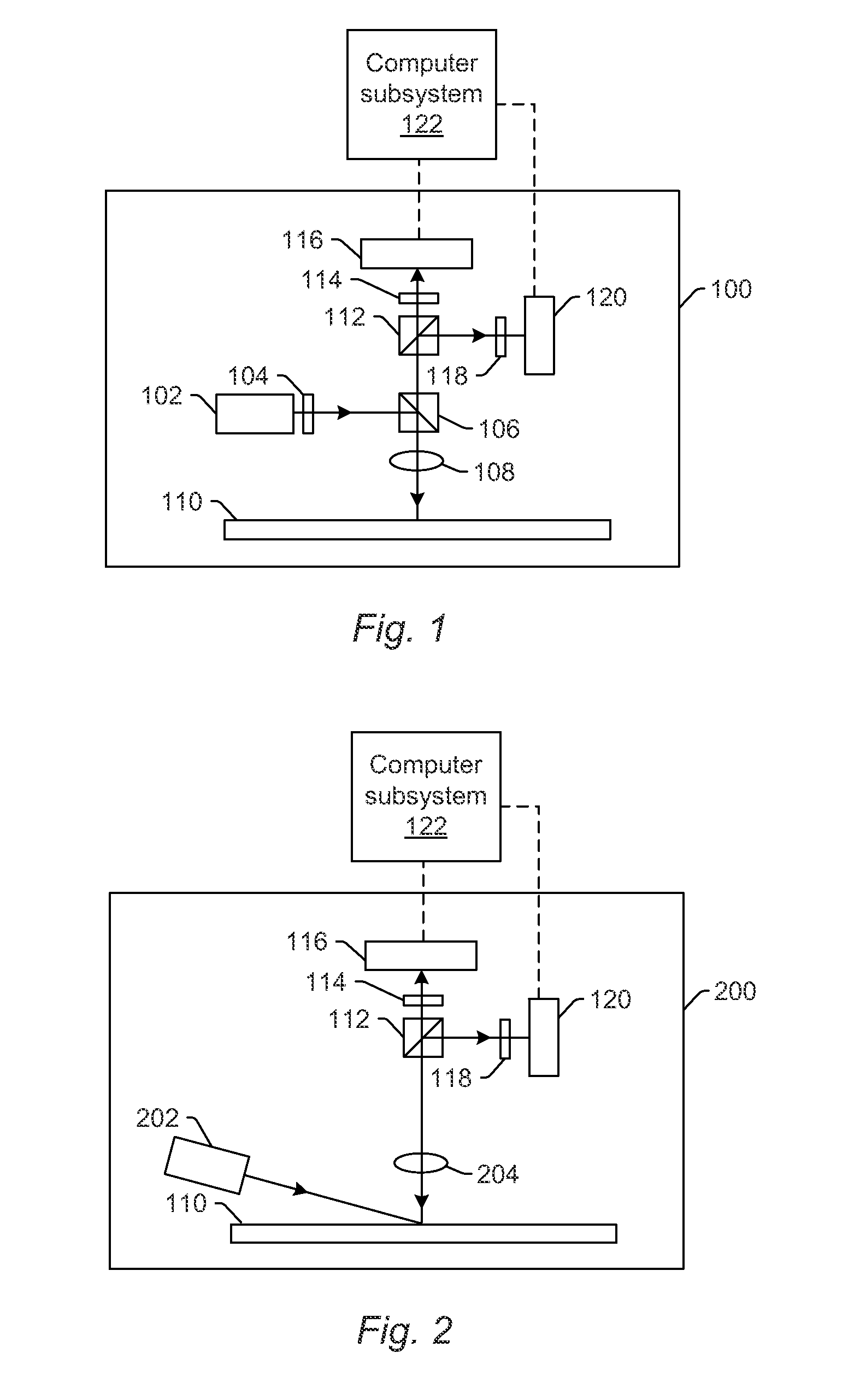
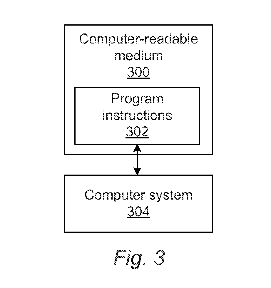
[0016]Turning now to the drawings, it is noted that the figures are not drawn to scale. In particular, the scale of some of the elements of the figures is greatly exaggerated to emphasize characteristics of the elements. It is also noted that the figures are not drawn to the same scale. Elements shown in more than one figure that may be similarly configured have been indicated using the same reference numerals. Unless otherwise noted herein, any of the elements described and shown may include any suitable commercially available elements.

[0017]One embodiment relates to a system configured to determine information for defects on a wafer. For example, the systems described herein can be used for defect detection and classification based on fluorescence detection from patterned wafers. In addition, the embodiments provide ways to enhance defect detection, characterization, and imaging for patterned wafers by the collection or rejection of fluorescence emitted by defects or patterns unde...


PUM

PropertyMeasurementUnit
wavelengthsaaaaaaaaaa
defectsaaaaaaaaaa
wavelengthsaaaaaaaaaa

Abstract

Systems and methods for determining information for defects on a wafer are provided. One system includes an illumination subsystem configured to direct light having one or more illumination wavelengths to a wafer. The one or more illumination wavelengths are selected to cause fluorescence from one or more materials on the wafer without causing fluorescence from one or more other materials on the wafer. The system also includes a detection subsystem configured to detect only the fluorescence from the one or more materials or to detect non-fluorescent light from the wafer without detecting the fluorescence from the one or more materials. In addition, the system includes a computer subsystem configured to determine information for defects on the wafer using output generated by the detection subsystem responsive to the detected fluorescence or the detected non-fluorescent light.

Description

BACKGROUND OF THE INVENTION[0001]1. Field of the Invention[0002]The present invention generally relates to systems and methods for determining information for defects on wafers.[0003]2. Description of the Related Art[0004]The following description and examples are not admitted to be prior art by virtue of their inclusion in this section.[0005]Inspection processes are used at various steps during a semiconductor manufacturing process to detect defects on wafers to promote higher yield in the manufacturing process and thus higher profits. Inspection has always been an important part of fabricating semiconductor devices such as ICs. However, as the dimensions of semiconductor devices decrease, inspection becomes even more important to the successful manufacture of acceptable semiconductor devices because smaller defects can cause the devices to fail.[0006]Some currently used inspection systems are configured to detect or suppress fluorescence signals from defects or wafer background. H...

Claims


Application Information

Patent Timeline
Patent Type & Authority Applications(United States)
IPC IPC(8): G01N21/95G01N21/94G01N21/64
CPCG01N21/9501G01N21/64G01N2201/12G01N2201/0612G01N21/94G01N21/6489
Inventor PALOMBA, STEFANOKOLCHIN, PAVELHAURYLAU, MIKHAILDANEN, ROBERT M.SHORTT, DAVID W.
Owner KLA CORP
Features
  • R&D
  • Intellectual Property
  • Life Sciences
  • Materials
  • Tech Scout
  • Unparalleled Data Quality
  • Higher Quality Content
  • 60% Fewer Hallucinations
Learn More