Touch display device

a display device and touch technology, applied in the field of touch display devices, can solve the problems of black matrix slightly conductive, light leakage or short circuit, resistance reduction, etc., and achieve the effect of preventing black matrix

Inactive Publication Date: 2015-06-04
INNOLUX CORP
View PDF10 Cites 9 Cited by
  • Summary
  • Abstract
  • Description
  • Claims
  • Application Information

AI Technical Summary

Benefits of technology

[0009]An object of the present invention is to provide a touch display device, which can prevent black matrix from electrostatic damage due to the charge accumulation on the surface with a smaller radius of curvature or sharp corners during the touch panel manufacturing process.
[0011]Accordingly, since the touch display device of the present invention has a larger spacing than conventional touch panels at the overlapping region, the charge on the electrode region will be evenly distributed and will not easily accumulate at some specific regions, thus preventing electrostatic damage during the manufacturing process of the touch panel and improving the process yield.

Problems solved by technology

However, in the manufacturing process of the touch panel, the backend-process temperature may carbonize the black matrix (BM) material and result in a reduced resistance, making the black matrix slightly conductive.
Therefore, when the charge continues to accumulate, a large voltage difference will be formed and electro-static discharge (ESD) will be induced to damage the black matrix, which ultimately results in the light leakage or short-circuit problem.

Method used


Image

  • Touch display device
  • Touch display device
  • Touch display device

Examples


example

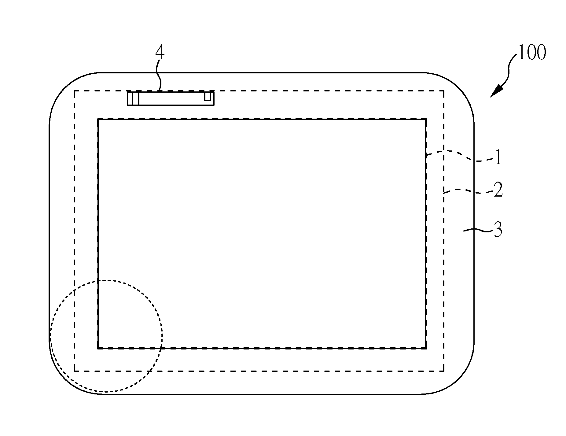
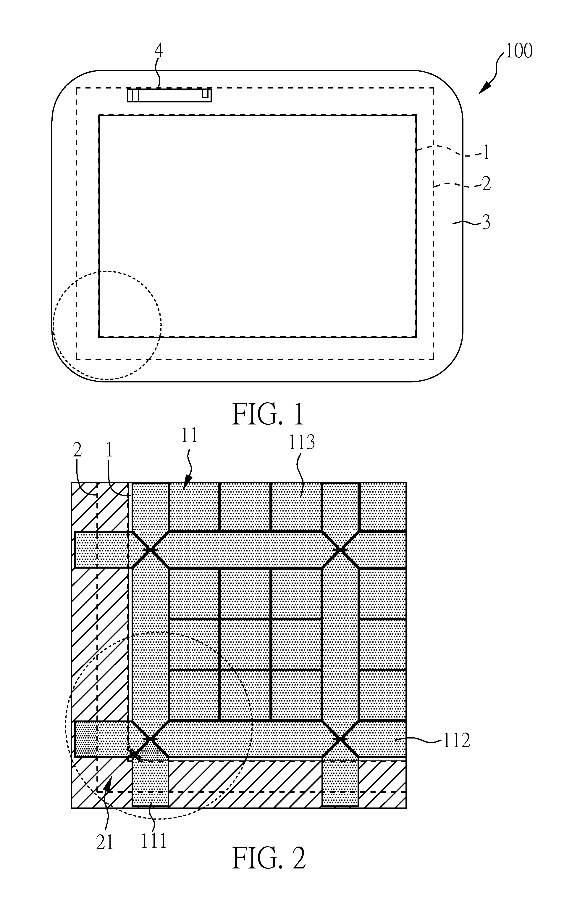
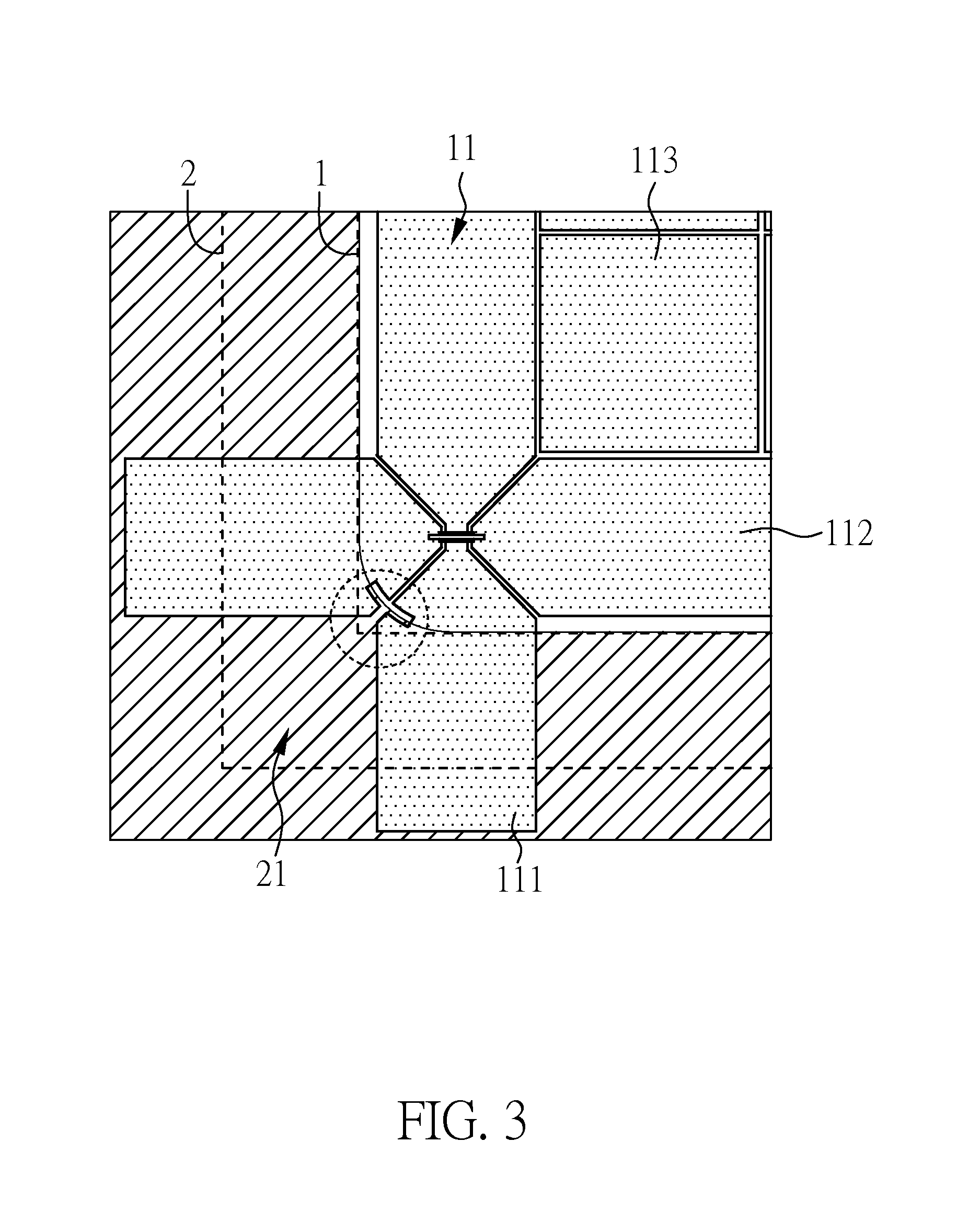
[0022]FIG. 1 shows a schematic diagram of the touch panel according to an embodiment of the present invention. As shown in FIG. 1, the touch panel 100 is divided into the sense region 1, the edge region 2, the frame 3 and the wiring region 4, wherein the enlarged view of the corner region (encircled by a dotted line) of the panel is shown in FIG. 2. Referring to FIG. 2, a wiring layer 11 of the touch panel 100 includes a first signal electrode 111, a second signal electrode 112, and a dummy electrode 113, and the wiring layer 11 is disposed above a shielding layer 21, wherein the enlarged view of the corner region (encircled by a dotted line) of the panel is shown in FIG. 3; and the enlarged view of portions (encircled by a dotted line) of the first signal electrode 111 and the second signal electrode 112 of FIG. 3 is shown in FIG. 4A.

[0023]Referring to FIG. 4A, the first signal electrode 111 includes a first non-overlap region 111A and a first overlap region 111B, and the second si...


PUM


Abstract

The present invention relates to a touch display device, comprising: a display device; and a touch panel disposed on a side of the display device, wherein the touch panel comprises: a substrate; a shielding layer disposed between the substrate and the display device; and a wiring layer disposed between the shielding layer and the display device, comprising: a first signal electrode comprising a first overlap region and a first non-overlap region; and a second signal electrode comprising a second overlap region and a second non-overlap region; wherein the first overlap region and the second overlap region overlap with the shielding layer; and a spacing between the first overlap region and the second overlap region is greater than a spacing between the first non-overlap region and the second non-overlap region.

Description

CROSS REFERENCE TO RELATED APPLICATION[0001]This application claims the benefits of the Taiwan Patent Application Serial Number 102143699, filed on Nov. 29, 2013, the subject matter of which is incorporated herein by reference.BACKGROUND OF THE INVENTION[0002]1. Field of the Invention[0003]The present invention relates to a touch display device, and especially to a touch display device which can prevent the black matrix from the internal electrostatic damaging.[0004]2. Description of Related Art[0005]Recently, with the development trend of user-friendly operation and simplicity, touch display devices are becoming more and more widely used in the production and life. Since the user can input signals directly by hand or other objects to access the touch display device, the user's dependence on other input devices (such as a keyboard, a mouse, a remote controller and so on) are thus reduced or even eliminated, thereby greatly facilitating the user's operation.[0006]The touch panel tech...

Claims


Application Information

Patent Timeline
Patent Type & Authority Applications(United States)
IPC IPC(8): G06F3/044
CPCG06F2203/04107G06F3/044G06F3/0443G06F3/0446
Inventor CHIEN, CHARLESCHU, I-CHIEH
Owner INNOLUX CORP
Why Eureka
Try Eureka